Introduction
Welcome to “The PC Emulation Book.”
This document aims to become a comprehensive guide to emulating the original models of the IBM Personal Computer:
- The IBM Model 5150 Personal Computer
- The IBM Model 5160 Personal Computer XT
When we refer to the original “IBM PC”, we are technically referring to the IBM Model 5150. However, the slightly improved IBM Model 5160 (otherwise known as the IBM XT) is similar enough in design and function that they are often lumped together. In this book, we will refer to the XT when a distinction between the PC and XT is important. Otherwise, consider any reference to the “PC” as referring to either model.
🚧 UNDER CONSTRUCTION! 🚧
You’ll notice that many of the pages in this book are empty stubs. Content is still being fleshed out. Here is a list of some of the more complete pages:
- The Intel 8253 Programmable Interval Timer
- The Intel 8259 Programmable Interrupt Controller
- The Keyboard
- The Keyboard Interface
- Display Concepts
Additionally, many of the appendices contain useful reference information:
Why Emulate the PC?
The IBM PC is arguably one of the most influential computers in history, establishing standards that enabled the proliferation of “PC-compatible” systems and cemented the very term “PC” as an Intel-based system, probably running a Microsoft operating system. The “PC” lives on even today, only recently challenged for supremacy by the rise of ARM-based CPUs.
The PC was an open and well-documented system. IBM published full schematics and commented BIOS source code listings, allowing anyone to understand in great detail how the system operated, even without owning the physical hardware.
There are thousands of software titles to explore on a PC emulator, although the PC’s limited graphics and sound capabilities make many of the games for the platform less than spectacular. Still, there are some classic titles that are still fun to play today, such as AlleyCat and Digger.
If you’re up for a challenge, recently several demos have been released that push the original PC hardware to its utter limits and require cycle-exact emulation of the 5150 and its components. These demos include 8088 MPH, released in 2015, and Area 5150, released in 2022.
Even without any attempt at cycle-accuracy, the PC can be emulated with a respectable level of compatibility.
What You’ll Learn
This book aims to cover the complete process of building a PC emulator from the ground up, including:
- Hardware Architecture: Understanding the IBM PC’s system design and component interactions
- CPU Emulation: Implementing the Intel 8088 processor
- Support Chips: Emulating the various Intel support chips that made the PC work
- Peripheral Devices: Implementing keyboards, displays, storage, and other I/O devices
- System Integration: Bringing all components together into a working emulator
Target Audience
This book is intended for emulator authors, but retro-developers may find it a useful reference as well, or anyone simply curious about how classic computers of the era worked.
Prerequisites
To get the most out of this book, you should have:
- A basic understanding of computer architecture concepts
- Familiarity with a high-performance programming language (C, C++, Rust, or similar)
- Basic electronics knowledge
- This is minimal, but you should understand the concepts of voltage, the function of resistors, and what a tri-state output is. If you need it, a refresher can be found in the appendices: Electronics Concepts.
- Basic understanding of digital logic
- Some experience with emulation
- If you have never programmed an emulator before, it is recommended that you start with the CHIP-8, a simple system that teaches basic emulation concepts. You can find a guide here.
License
This book is open-source and all content is licensed under the Creative Commons CC BY 4.0 license, except where otherwise noted. See LICENSE.
Acknowledgements
Several resources have been invaluable references in both my development of my emulator and in curating material for this book. I would like to thank the following for graciously providing permission to directly adapt or include their work:
- modem7 of minuszerodegrees.net
- Scott Smitelli of cosmodoc.org
- Francis Gulotta of roborooter.com
Other invaluable resources for PC information include:
- John Elliott’s seasip.org
- Ken Shirriff’s blog at righto.org
- Reenigne’s blog at reenigne.org
- Great Heirophant’s blog at nerdlypleasures.blogspot.com
- VileR’s int10h.org
Contributing
The main source repository for the PC Emulation Book can be found here. PRs are welcome.
AI Policy
The PC Emulation Book strives to maintain accurate and authentically voiced information. To that end, all content contributed to the PC Emulation book should be written by human beings. Don’t worry if English is not your first language - I will be glad to perform editorial duties for you.
IBM PC/XT Architecture Overview
The design of the original IBM 5150 reflected IBM’s project requirements to create a low-cost, maintainable system largely comprised of off-the-shelf parts, yet capable of being expanded. They succeeded in that effort far beyond any conceivable expectations - the IBM PC is now recognized as the ancestor of a line of “PC Compatible” systems that continue to be sold to this day.
CPU
IBM chose the Intel 8088 for the 5150, which is also used in the 5160. The 8088 was a lower-cost variant of the 8086 CPU. While still 16-bit internally, the 8088 only had an 8-bit data bus. This simplified the PC’s motherboard design, and made it easy to build a system around Intel’s various 8-bit peripheral chips.
The 8088 has 20 address lines, allowing it to address \(2^{20}\) bytes, or 1MB.
IBM chose to reserve addresses above 0xA0000, leading to the infamous “640KiB” memory limit that is often mistakenly blamed on Microsoft.
Memory
Depending on the model and revision, the PC could be fitted with up to 256K of RAM on the motherboard. Memory expansion cards to bring a system up to the maximum 640KiB were quite commonplace in the latter years of the PC’s life. Multi-function cards provided RAM upgrades along with extra peripherals such as printer, serial, and game ports.
The memory used in the PC is common dynamic RAM (DRAM). The PC lacks dedicated refresh circuitry to maintain the contents of DRAM, and must use some of its accessory hardware to perform this task. The process of DRAM refresh makes the entire system approximately 6% slower.
Timer
The PC contains an Intel 8253 Programmable Interrupt Timer with three timing channels.
Timer Channel 0
The first channel, 0, is dedicated to maintaining the system clock via the BIOS. The PC has no real-time clock or battery-backup, so the date and time must be entered when booting the system. The time-of-day clock is maintained in software, and was notoriously inaccurate. For these reasons, real-time clock modules were popular upgrades, often found on multi-function cards. Timer channel 0 is connected to IRQ0 and is the only channel that can generate *timer interrupts.
Timer Channel 1
The second channel, 1, is dedicated to the operation of refreshing the system’s DRAM and generally cannot be used by programs.
Timer Channel 2
The third channel, 2, is the only channel connected to the PC Speaker. Programming this channel allows sounds to be played, but it can also be used as a general timing facility.
DMA
The PC has an Intel 8237 Direct Memory Access Controller. DMA is a method by which expansion cards can read and write to memory without needing the CPU to participate in the transfer, which can make timing-critical operations such as floppy-disk access more reliable, especially if the CPU is busy. DMA was used to operate the PC’s floppy drives, and was often used by add-on hard disk controllers. The PC has three DMA channels, one of which is dedicated to the process of DRAM refresh, leaving only two available.
Interrupts
The PC has an Intel 8259 Programmable Interrupt Controller with 8 interrupt lines. Interrupts are a way for components of a hardware system to request attention from the CPU.
Expansion Bus
The 8-bit data bus of the 8088 would also dictate the 8-bit data width of the system’s expansion bus. This bus would later be expanded to 16-bits with the IBM 5170 AT, and would later be dubbed the ISA bus by Compaq1 and a growing consortium of PC clone manufacturers.
System Crystal
The 5150 has a single main system crystal with a frequency of 14.31818MHz. This frequency is exactly four times the NTSC color subcarrier frequency.
The crystal frequency can be expressed as a fraction:
$$f_{crystal} = \frac{315}{22} \text{ MHz} = 14.31818\overline{18} \text{ MHz}$$
This choice was likely made due to the low cost of NTSC-derived clock crystals, as they were being manufactured by the millions to be used in television sets. It also made the PC more easily compatible with North American television sets, making low-cost display option available to PC owners. It also allowed the IBM Color Graphics Adapter to omit a separate crystal.
CPU Clock
The CPU frequency of 4.77 MHz is obtained by dividing the system clock by 3:
$$\frac{14.3181818}{3} = 4.773\text{ MHz}$$
The 8088 was rated for 5MHz operation2, so this represents about a 5% underclock.
The PC vs XT
The IBM model 5160 (XT) is very similar to the model 5150 PC, with a few differences:
- Eight expansion slots vs the PC’s five
- The minimum installed RAM was increased to 128K
- The underutilized cassette interface port was dropped
- Slight changes to DRAM refresh logic
- ROM chip size was increased from 8K to 32K
- A larger, 130W power supply to accommodate hard drives
References
-
wikipedia.org Industry Standard Architecture. ↩
-
Intel Corporation. 8088 8-Bit Hmos Microprocessor. Intel Corporation, August 1990. Document Number: 231456-006. Available at: Intel 8088 Data Sheet PDF ↩
Intel 8088 CPU
Architecture and Registers
Instruction Set and Execution
Bus Interface and Timing
Intel 8259 Programmable Interrupt Controller
The Intel 8259 Programmable Interrupt Controller (PIC) plays an essential role in the operation of much of the hardware of the IBM PC. The PIC can be thought of as an expansion unit to the 8088’s single INTR pin, allowing 8 separate interrupt sources to be handled in a prioritized manner.
The PIC is a surprisingly challenging chip to emulate correctly, partially due to some ambiguities in its documentation.
Overview
The 8 inputs of the PIC are called Interrupt Request lines, which are often referred to as IRQs (Interrupt reQuest).
The PIC has three main 8-bit registers. Each bit in these registers corresponds to an IRQ with the least significant bit mapping to IRQ 0 and the most significant bit mapping to IRQ 7.
- Interrupt Request Register (IRR): This register holds bits reflecting the IRQ lines that are requesting service.
- Interrupt Mask Register (IMR): A
1bit set in this register prevents the corresponding IRQ line from being serviced. - In-Service Register (ISR): A
1bit set in this register indicates that the corresponding IRQ has been acknowledged by the CPU and is now “in-service”.
The 8 IRQs of the PIC are ordered in terms of priority, with IRQ 0 being the highest priority, and IRQ 7 being the lowest priority. This means that if IRQ 0 and IRQ 1 occur simultaneously, IRQ 0 will be serviced first.
This also means that it is possible for a higher priority interrupt to be serviced while a lower priority interrupt is already in service. Normally, the 8088 clears the I flag when executing an interrupt. If a programmer desires their interrupt service routine to be reentrant, they would need to issue an STI instruction to allow this to occur.
IBM PC PIC Configuration
IRQ Assignments
The IBM PC maps devices to the 8259’s IRQ lines as follows. Some of these connections are direct traces on the motherboard, other IRQs are connected to the ISA bus. In some cases, a peripheral card may have had a jumper to allow selection of a particular IRQ.
| IRQ | Connection | Device |
|---|---|---|
| IRQ 0 | Direct | System Timer |
| IRQ 1 | Direct | Keyboard Controller |
| IRQ 2 | ISA/Direct | Vsync Interrupt (EGA) or Secondary 8259 (AT) |
| IRQ 3 | ISA | Serial Port - COM2 |
| IRQ 4 | ISA | Serial Port - COM1 |
| IRQ 5 | ISA | Hard Disk Controller or LPT2 |
| IRQ 6 | ISA | Floppy Disk Controller |
| IRQ 7 | ISA | Parallel Port - LPT1 |
I/O Ports
The 8259 has a single address pin, A0, via which one of two registers can be selected.
The two registers are decoded by the PC at the following addresses:
| PC Port | 8259 Port | RW | Description |
|---|---|---|---|
| 0x20 | 0 | RW | Command/Status Register |
| 0x21 | 1 | RW | Data/Mask Register |
The Unimportant Stuff
The 8259 was designed to be compatible not only with the 8088 and 8086, but with Intel’s earlier CPUs, the 8080 and 8085. There are various mode flag bits that control whether the 8259 should expect to be paired with an 8088 or not - obviously, on the IBM PC, you can expect these bits to be set properly, and emulation of the 8080 modes is certainly not required.
The 8259 supported daisy-chaining of additional 8259 chips to enable more interrupt sources to be handled - something that Intel called cascading. This was not used on the IBM PC, which only had a single 8259. Two 8259s were employed on the IBM 5170 AT in a primary/secondary configuration. Obviously this is something you do not need to emulate either.
The PIC can be operated in edge-triggered or level-triggered mode. The IBM PC exclusively operates in edge-triggered mode, but implementing level-triggered mode is fairly trivial to do.
There are additional features like priority rotation and special mask mode which are not used by the IBM PC.
Interrupt Processing Logic
The important thing to understand about the PIC is that it is implemented as an array of 8 priority cell circuits. The IRR, IMR, and ISR “registers” are simply latches within each priority cell. This means that a good part of the interrupt evaluation logic happens continuously, since it is simply driven by immediate state of the circuit. The PIC has no clock input, so all it can do is respond to changes of its input pins. With one exception - but we’ll talk about that later.
Let’s look at an example of interrupt logic flow:
The Simple Version
- A device raises its IRQ line connected to the PIC.
- The PIC looks to see if that IRQ is masked off in the IMR, if it is already in service, or if a higher-priority interrupt is in service, in which case the interrupt cannot be serviced at the moment.
- If the IRQ can be serviced, the PIC raises the INTR line to the CPU.
- The CPU acknowledges the interrupt and the PIC sets the corresponding bit in the ISR to indicate that the interrupt is now in service. The corresponding bit in the IRR is cleared to indicate the IRQ is no longer requesting service.
- The CPU executes the interrupt based on the 8-bit vector the PIC provides in response to the CPU’s interrupt acknowledgement.
- The interrupt service routine executes. When it is done, it sends an
End-of-Interrupt (EOI)command to the PIC. - The PIC clears the corresponding bit in the
ISRindicating that the interrupt has completed servicing.
The original IRQ line may remain high at this point, but in the PC’s standard edge-triggered mode it will not be serviced again until it transitions low and then high again.
The Detailed Version
- A device raises its IRQ line connected to the PIC.
- The low-to-high transition of the IRQ line sets the IRQ’s edge latch and sets the corresponding bit in the
IRR.- If the corresponding bit in the
IMRis set, the signal from theIRRdoes not propagate further. - If the corresponding bit in the
IMRis clear, the signal from theIRRreaches thePriority Resolver.
- If the corresponding bit in the
- The priority resolver checks to see if the corresponding bit in the
ISRis set, or if any bits lower than the corresponding bit are set, indicating a higher priority interrupt is already in service.- If any of these bits are set, nothing further happens for the moment.
- If none of these bits are set, the priority resolver will instruct the control logic to raise the PIC’s INTR pin, which is connected to the CPU.
- The CPU finishes an instruction, at which point it samples the INTR pin.
- The CPU notices INTR is high.
- If the CPU’s
Iflag is cleared, it ignores INTR being high and continues execution as normal.
- If the CPU’s
- The CPU begins to acknowledge the interrupt.
- The CPU issues one bus cycle with the
INTAbus status encoded. - The CPU bus controller decodes the
INTAbus status and asserts the physical \(\overline{INTA}\) pin.
- The CPU issues one bus cycle with the
- The PIC detects the \(\overline{INTA}\) pin going high.
- The priority resolver sets the highest-priority bit in the
ISRto indicate that the interrupt is entering service. - In edge-triggered mode, the priority resolver clears the corresponding bit in the
IRR.
- This is the only difference between edge-triggered mode and level-triggered mode.
- The control logic asserts the internal \(\overline{FREEZE}\) signal. This prevents any change to any bit in the
IRRwhile the interrupt acknowledge process is active.
- The priority resolver sets the highest-priority bit in the
- The \(\overline{INTA}\) pin goes low as the CPU completes the INTA bus cycle.
- The \(\overline{INTA}\) pin goes high again as the CPU issues a second INTA bus cycle.
- The PIC emits the 8-bit interrupt vector which the CPU reads during the second INTA bus cycle.
- The \(\overline{INTA}\) pin goes low as the CPU completes the second INTA bus cycle.
- The control logic de-asserts the \(\overline{FREEZE}\) signal, allowing the
IRRto update again. - In auto-EOI mode, the priority resolver clears the corresponding
ISRbit.
- The control logic de-asserts the \(\overline{FREEZE}\) signal, allowing the
- The CPU uses the interrupt vector received from the PIC to look up a far pointer to the correct Interrupt Service Routine from the Interrupt Vector Table.
- The CPU clears the
IandTflags, then jumps to the interrupt service routine. - At the end of the interrupt service routine, the routine sends an
EOIcommand to the PIC. - The PIC clears the appropriate bit in the
ISRto indicate that the interrupt has completed servicing.
The Intel 8253 Programmable Interval Timer
The 8253 Programmable Interval Timer (PIT) is responsible for a number of tasks on the IBM PC. It maintains the system time, drives DRAM refresh, and controls the PC speaker to generate sound.
Overview
The PIT contains three independently operating 16-bit counters or ‘channels’, each capable of operating in different modes.
Physically, each timer channel is assigned a clock input, a gate pin, and an output pin (OUT). The gate pin can be used to control or disable counting in specific modes.
Counters are operated by first configuring them by writing a Control Word to the 8253’s Control Word Register. Then, an initial count - often referred to as a ‘reload value’ - is written directly to the timer channel port. A counter has a full 16-bit range, as an initial count of 0 is treated as a count of 65,536 in binary mode or \(10^4\) in BCD mode.
Once configured and running, on each tick of the channel’s clock input, the channel’s internal Counting Element decrements. When the counter reaches 0 (or 1 in some modes), some specific behavior will be triggered (depending on mode), usually changing the state of the channel’s output pin.
The current value of a counter channel can be read at any time by reading from the channel’s specified port.
Pinout
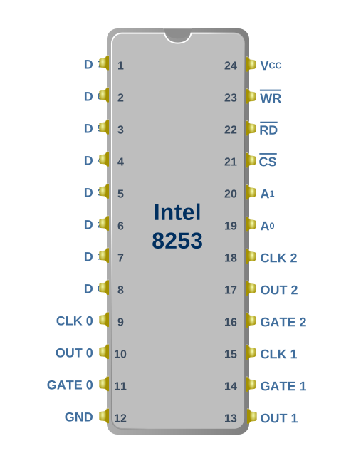
Figure 1: Intel 8253 Pinout
The 8253 has an 8-bit data bus by which you read and write the chip’s registers, which are selected by the A0 and A1 pins.
IBM PC Timer Configuration
The 8253 has three independent clock input pins, allowing each counter to be driven at a different frequency. The IBM PC ties all three clock inputs to the same clock line, which runs at the system crystal frequency divided by 12.
$$f_{timer} = \frac{\frac{315}{22}}{12} \text{ MHz} = 1.19318\overline{18} \text{ MHz}$$
Note: Other systems that use the 8253 can connect these timer clock inputs in different ways - even connecting one timer channel output to the clock input of another to act as a clock divisor.
| Timer | Purpose | Frequency | Connection |
|---|---|---|---|
| Timer 0 | System Timer | 18.2 Hz | System Timer Interrupt |
| Timer 1 | DRAM Refresh | 15 μs | DMA Controller for memory refresh |
| Timer 2 | Speaker | Variable | PC Speaker output |
Timer 0
Timer 0’s OUT pin is directly connected to the IR0 pin of the 8259A Programmable Interrupt Controller. When the Timer 0 OUT pin has a low-to-high transition, this will trigger an IRQ0. This causes an interrupt 8, which normally is configured to maintain the system’s time of day clock by the BIOS.
The BIOS initializes Timer 0 to a reload value of 0 (65,536)
$$ T = \frac{65536}{1.19318\overline{18}\times 10^{6}} \approx 0.0549254\ \text{s} $$
$$ T \approx 54.93\ \text{ms} $$
$$ \frac{1\text{s}}{54.93\text{ms}} \approx 18.2Hz $$
This will cause an Interrupt 8 to execute 18.2 times per second.
Many applications, especially games, will use Timer 0 for their own purposes, and so the time of day clock was notoriously inaccurate without being synchronized to a realtime clock module.
Timer 0’s GATE pin is tied to +5v.
Timer 1
Timer 1’s OUT pin connects to a 74LS74 flip-flop which latches its output. The output of this flip flop is connected to the DRQ0 pin of the 8237 DMA Controller, and is reset by the \(\overline{\text{DACK0}}\) signal. This causes one DMA transfer to occur in read mode, which refreshes the system’s DRAM.
The BIOS initializes Timer 1 to a reload value of 18:
$$ T = \frac{18}{1.19318\overline{18}\times 10^{6}} \approx 0.0000151\ \text{s} $$
$$ T \approx 15.1\ \text{μs} $$
$$ \frac{1\text{s}}{15.1\times 10^{-6}\text{s}} \approx 66.2\text{KHz} $$
This will cause a DMA refresh request approximately every 15 microseconds, or every 72 clock cycles. If this sounds like a lot, it is. The DRAM refresh process robs the 8088 of about 5-6% of its performance, depending on bus activity.
Note: You can ignore this channel if you are not interested in cycle-accuracy. However, the IBM PC BIOS does check that Timer 1 is running by checking that the DMA channel 0 is counting. You can hack your way around this test by just making the DMA channel 0 count on read.
Timer 1’s GATE pin is tied to +5v.
Timer 2
Timer 2’s OUT pin connects to the PC’s speaker and cassette interface circuitry. Timer 2 is typically configured to produce square waves to drive the speaker to play notes of specific frequencies, and Timer 2’s GATE input can be used to silence the speaker when desired.
For more details, see the PC Speaker chapter.
Timer 2’s GATE pin is tied to the 8255 PPI’s Port B, Bit 0 (Pin #18).
I/O Ports
The 8253 has two address lines, A0 and A1, which allow selection of four ports.
These four ports are decoded by the PC at the following addresses:
| PC Port | 8253 Port | RW | Description |
|---|---|---|---|
| 0x40 | 0 | RW | Timer 0 Count Register |
| 0x41 | 1 | RW | Timer 1 Count Register |
| 0x42 | 2 | RW | Timer 2 Count Register |
| 0x43 | 3 | W | Control Word Register |
Control Word Format
The 8253’s control word can be written to at port 0x43 and is used to configure one of the three counters, each of which can be configured with different modes.
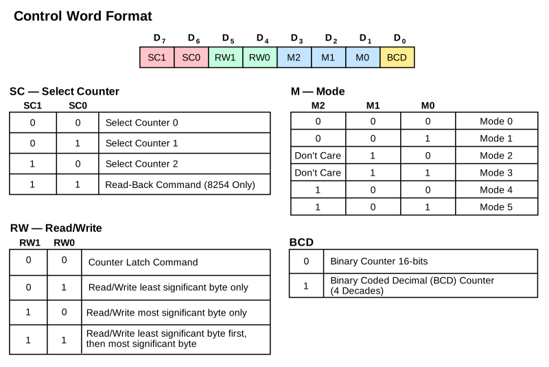
Figure 2: Intel 8253 Control Word Format
The specified channel’s counting mode, IO mode, and whether or not it should count in BCD, is configured with a single 8-bit write. Note that using 0b11 as the timer selection is invalid on the 8253. On the 8254, it selects the read-back command, which will not be covered here.
Counter Channel Configuration
Binary vs BCD Mode
A timer channel can be configured to count in either binary or Binary Coded Decimal (BCD) mode. I have not seen any software that actually uses BCD mode. When writing your initial 8253 implementation, you can probably ignore BCD mode.
RW Mode
A timer channel can be configured for 16-bit read/writes in LSBMSB mode using 0b11 in the RW field, or in one of two 8-bit read/write modes:
LSB(0b01):- On write, an 8-bit value is used to initialize the \(\text{CR}_l\) register, which holds the least significant 8 bits of the initial 16-bit count.
- On read, the contents of the \(\text{O}_l\) register are returned. See Counter Channel Operation.
MSB(0b10):- On write, an 8-bit value is used to initialize the \(\text{CR}_m\) register, which holds the most significant 8 bits of the initial 16-bit count.
- On read, the contents of the \(\text{O}_m\) register are returned. See Counter Channel Operation.
The 8-bit RW modes allow programming a timer channel with fewer writes. In MSB mode, the full range of a timer channel is available, with reduced granularity.
Note: The RW mode of a channel does not affect its basic counting operation. It remains a full 16-bit counter internally regardless of input mode.
In LSBMSB mode, it takes two 8-bit writes to read or write to the timer channel. An internal latch keeps track of whether the initial LSB has been written. On a write, the first byte written is used to initialize the \(\text{CR}_l\) register. The second byte initializes the \(\text{CR}_m\) register. On a read, the first read returns the \(\text{O}_l\) register, the second read returns the \(\text{O}_m\) register.
Warning: The 8253 cannot handle interleaved 16-bit read and write operations. In
LSBMSBmode if you write one byte and then read one byte without completing the write operation, you will receive random data. Some software has been observed improperly operating the 8253 in this way, especially software designed for the 8254 which did not have this limitation. Ensure that your 8253 can recover in this scenario - what value you decide to return is up to you - the actual value is nondeterministic “open bus” behavior internal to the chip.
Counter Latch Command
There is a small matter of concern when a channel is configured for LSBMSB mode. Since it takes two bytes to read the full 16-bit counter value, it is possible that the counter can decrement between the time the first byte is read and the second. Therefore, a Counter Latch command is provided. The Counter Latch command is sent by setting the RW field of the control word to 0b00. This does not change the counter channel’s configuration otherwise - the Mode and BCD bits are ignored when sending the counter latch command. See the Counter Latch Operation section below for how the latching is implemented.
Counter Channel Operation
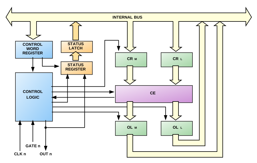
Figure 3: Intel 8253 Counter Block Diagram
There are a few important things to note in the channel block diagram above. The heart of the counter is the Counting Element (CE). This is a 16-bit synchronous down-counter that contains the current count value. Above the CE are \(\text{CR}_m\) and \(\text{CR}_l\), two halves of the Count Register (CR). The CR holds the initially configured count, and is used to reload the CE on terminal count in modes that do so.
The count value is transferred from the CR to the CE when a full write of the CR is complete. This may require one or two bytes, depending on the configured RW Mode.
Both Count Registers are initialized to 0 whenever a channel’s mode is set. This avoids leaving either of the CR registers in an indeterminate state when using either byte RW mode.
Counter Loading
Counter loading is not instantaneous on write. A CR is not loaded until the 8253 sees a full clock cycle with a rising and falling edge after the write occurs. If the specific mode requires that the CE be loaded immediately from the CR, all 16-bits are transferred at once.
A count can be loaded with any 16-bit value from 0-65,535. To allow a full 16-bit range, a count value of 0 is interpreted by the 8253 as a count value of 65536.
Counter Latch Operation
Below the CE are \(\text{O}_m\) and \(\text{O}_l\), two halves of the Output Latch. When reading the count value from a channel, we are actually reading from the output latch. Typically, the output latch is updated each time the CE changes. When the Counter Latch Command is issued, the CE simply stops updating the Output Latch, essentially “freezing” the value inside at the point in which the latch command was issued.
When the Output Latch is fully read, which may take one or two bytes depending on the configured RW Mode, the Output Latch is “unfrozen” and will resume being updated by the CE on every tick.
The Output Latch operation can only be reset by fully reading the Output Latch. Issuing a new Counter Latch command will be ignored until the Output Latch is fully read.
Clocking Logic
An 8253 timer channel generally takes an action, such as transferring the CR to CE or decrementing the CE on the next falling edge of its input clock.
Counter Operating Modes
Timer channels can be set to any of 6 different modes.
- Mode 0: Interrupt on Terminal Count
- Mode 1: Hardware Retriggerable One-Shot
- Mode 2: Rate Generator
- Mode 3: Square Wave Generator
- Mode 4: Software Triggered Strobe
- Mode 5: Hardware Triggered Strobe (Retriggerable)
Mode 0 — Interrupt on Terminal Count
Upon setting this mode, OUT is initially LOW. This is the only mode where the initial OUT state is LOW after a mode is set.
In Mode 0, the counter counts down once per tick from the initial count until it reaches 0. When it reaches 0, OUT goes high and stays high until reprogrammed. The counter will continue to count, rolling over from 0 to 0xFFFF, but no longer affects the state of the OUT pin.
Note: The word “Interrupt” in this mode name can be a little misleading. Nothing about this mode is specific to generating interrupts. Interrupts are generated whenever timer channel 0’s output has a rising edge. Therefore, any operating mode can generate interrupts with timer channel 0. Additionally, using the Interrupt on Terminal Count mode on any other timer channel will not generate an interrupt.
Count Loading
- After setting the mode and initial count, the CR will be loaded into the CE on the next clock edge after the final write of the initial count.
Output Behavior
- After mode set: OUT → LOW
- When countdown reaches 0: OUT → HIGH (and remains HIGH)
- Upon writing new count: OUT → LOW
GATE Behavior
- Level-triggered
- GATE HIGH: enables counting
- GATE LOW: inhibits counting (freezes the countdown)
Reload Behavior
- In 8-bit RW modes:
- Writing either the
LSBorMSBwhile the counter is running forces OUT low immediately. - The CR will be loaded into the CE on the next clock edge.
- Writing either the
- In
LSBMSBRW mode:- Writing the
LSBwhile the counter is running disables counting and forces OUT low immediately. - Writing the
MSBwill load the CR into the CE on the next clock edge.
- Writing the
Timing
- For initial count = N, OUT will go high up to N+1 timer clock cycles after the write.
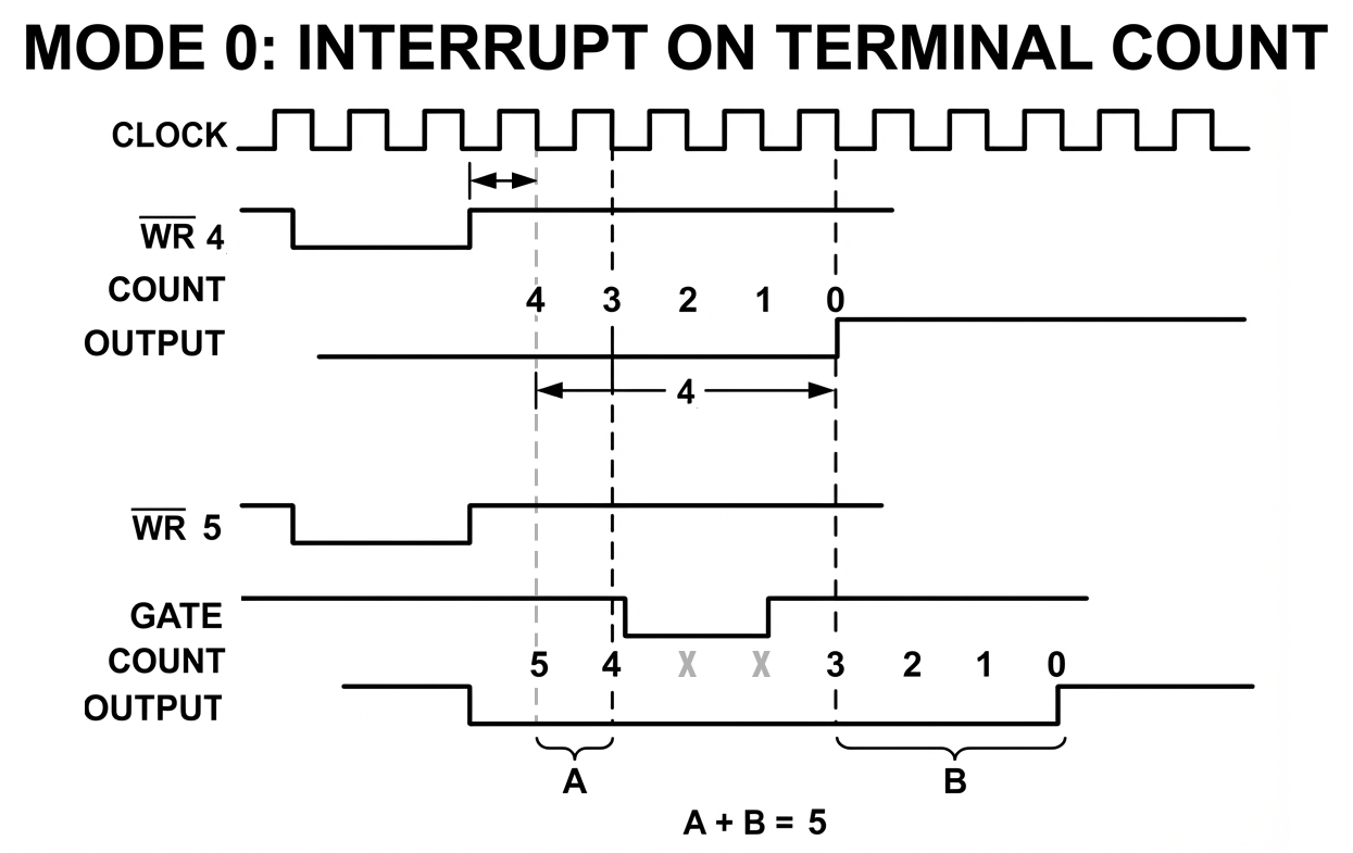
Figure 4: Timer Mode 0 - Interrupt on Terminal Count Timing
Mode 1 — Hardware Retriggerable One-Shot
Summary
This mode allows a low pulse of the OUT pin of a configurable length, triggerable via the GATE pin. This mode is inoperable on the IBM PC except on timer channel 2.
Upon setting this mode, OUT is initially HIGH. A rising edge of the GATE input will trigger OUT → LOW on the next clock edge. When the count reaches 0, OUT → HIGH. The counter will continue to count, rolling over from 0 to 0xFFFF, but will not affect the state of the OUT pin until the counter is re-triggered.
We refer to a “trigger” as a LOW → HIGH transition of the GATE pin.
Note: The count starts running as soon as Mode 1 is selected - but you’ll note that the CE is not loaded until a GATE trigger. Presumably, the counting element still contains whatever it had in it when the mode was set, but this has not been verified.
Count Loading
- After setting the mode and initial count, the CR will hold the initial count but will NOT write it into the CE until a trigger occurs.
Output Behavior
- After mode set: OUT → HIGH
- After GATE LOW → HIGH: OUT → LOW
- At terminal count: OUT → HIGH
GATE Behavior
- Edge-triggered
- GATE LOW -> HIGH: Trigger. The CR is loaded into the CE on the next clock edge.
- Since the trigger reloads the CE, another trigger will restart any count in progress.
Reload Behavior
- Writing a new count during an active count will not affect the current count until the next trigger, as the trigger controls loading of the CE from CR.
Timing
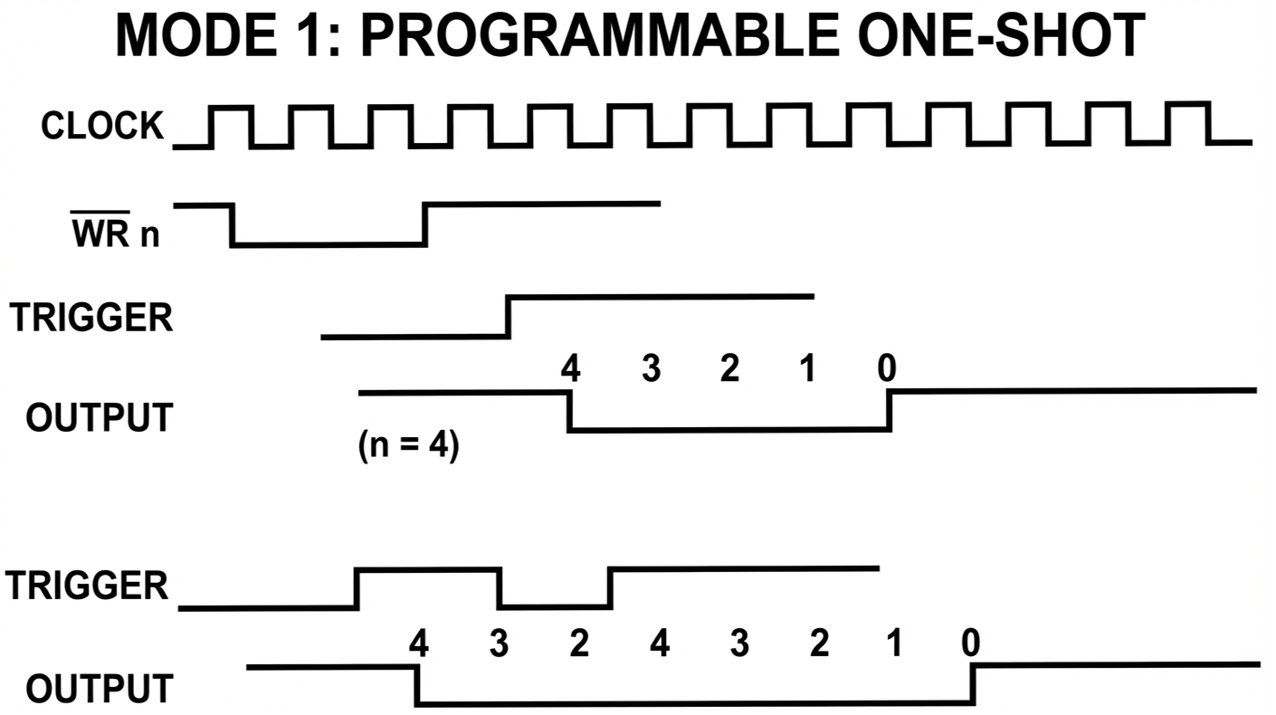
Figure 5: Timer Mode 1 - Hardware Retriggerable One-Shot Timing
Mode 2 — Rate Generator
Summary
In this mode, OUT normally remains HIGH, but produces regular one-clock-wide low pulses. This mode is useful when a periodic LOW → HIGH transition is required.
On the IBM PC, timer channel 1 is typically configured for Mode 2 to repeatedly generate the \(DREQ0\) signal.
Output Behavior
- After mode set: OUT → HIGH
- When count reaches 1: OUT → LOW
- When count reaches 0: OUT → HIGH
GATE Behavior
- Edge-triggered
- GATE LOW -> HIGH: Trigger. The CR is loaded into the CE on the next clock edge. Counting enabled.
- GATE LOW: OUT is forced HIGH, counting disabled.
Reload Behavior
- Writing a new count during an active count will not affect the current count until either a terminal count or a GATE trigger.
- CR is automatically loaded into the CE after terminal count is reached, restarting the count.
Constraints
- A count of 1 is invalid and will cause the timer channel not to function.
Timing
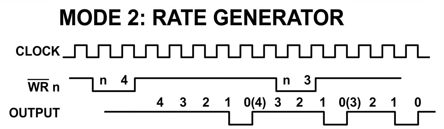
Figure 5: Timer Mode 2 - Rate Generator Timing
Mode 3 — Square Wave Generator
Summary
Similar to Mode 2, but produces a square wave: OUT alternates high and low with a 50% duty cycle (if the initial count is even). This is a general-purpose mode with many applications. The IBM BIOS sets timer channel 0 to Mode 3 to run the BIOS time-of-day clock. This mode can also be used to drive a tone of a specific frequency to the PC speaker on timer channel 2.
This mode is a bit more complex than the other modes. The 8253 creates a square wave of a period determined by the initial count by decrementing the counting element by 2 instead of 1. This presents a problem if the initial count is odd, as we need to reach 0 to trigger the terminal count condition.
Odd Count Logic
Within the counter is a flip-flop I will call the 1/3 flip-flop. This flip-flop is initially 0.
- If the CE is odd, the 8253 will decrement it as follows:
- If the 1/3 flip-flop is 0, the CE will be decremented by 1. This sets the CE to an even value.
- If the 1/3 flip-flop is 1, the CE will be decremented by 3. This sets the CE to an even value.
- If the CE is even, the 8253 will decrement it by 2.
- When the counter reaches terminal count (0), CE is reloaded by CR, and the 1/3 flip-flop is toggled.
This is a somewhat awkward way of accounting for the one missed clock period per cycle we would otherwise accumulate over time with an odd count. The result of this logic is that the resulting square wave is HIGH for \(\frac{N+1}{2}\) clocks and LOW for \(\frac{N-1}{2}\) clocks.
Note: The 8254 implements the logic for Mode 3 differently than the 8253. Refer to the 8254 datasheet for an accurate description if you are emulating an 8254.
The counter also has an output flip-flop that it uses in this mode to toggle the state of the OUT pin when terminal count is reached.
Output Behavior
- After mode set: OUT → HIGH
- At terminal count: OUT toggles state
GATE Behavior
- Edge-triggered
- GATE HIGH: Trigger. The CR is loaded into the CE on the next clock edge. Counting enabled.
- GATE LOW: OUT → HIGH. Counting disabled.
Reload Behavior
- Writing a new count during an active count will not affect the current count until either a terminal count or a GATE trigger.
- CR is automatically loaded into the CE after terminal count is reached, restarting the count.
Timing
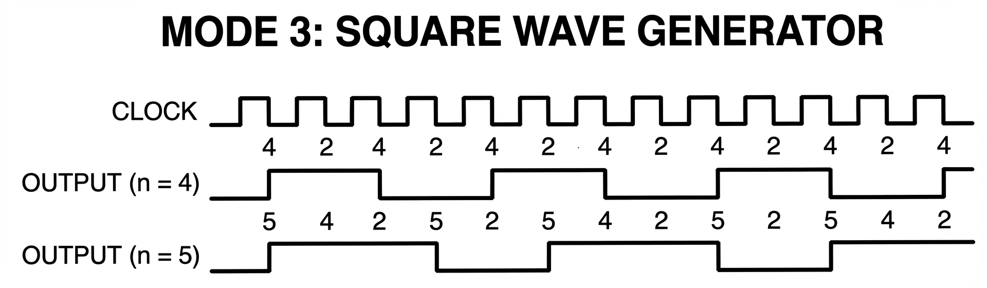
Figure 6: Timer Mode 3 - Square Wave Generator Timing
Mode 4 — Software Triggered Strobe
Summary
When the initial count reaches 0, OUT produces a one-clock-wide low pulse. This is similar to Mode 2, but with a distinct difference - in Mode 2, OUT goes low on a count of 1, and HIGH again on a count of 0. In Mode 4, OUT goes low on a count of 0, then HIGH again on the next clock edge. The counter will continue to count, rolling over from 0 to 0xFFFF, but will not affect the state of the OUT pin until the next count value is written.
Counting begins when the initial count is written (the “software trigger”).
Output Behavior
- After mode set: OUT → HIGH
- At terminal count: OUT → LOW for one clock period
Count Loading
- After writing the count, the CR is loaded into the CE on the next clock edge. Counting begins automatically on the following clock edge.
- Writing a new count during an active count will trigger a CR to be loaded into the CE at the next clock edge.
- In
LSBMSBmode, writing the first byte only has no effect.
- In
GATE Behavior
- Level-triggered
- GATE HIGH: Counting enabled.
- GATE LOW: Counting disabled.
- GATE does not affect OUT.
- GATE does not trigger a reload of the counter.
Timing
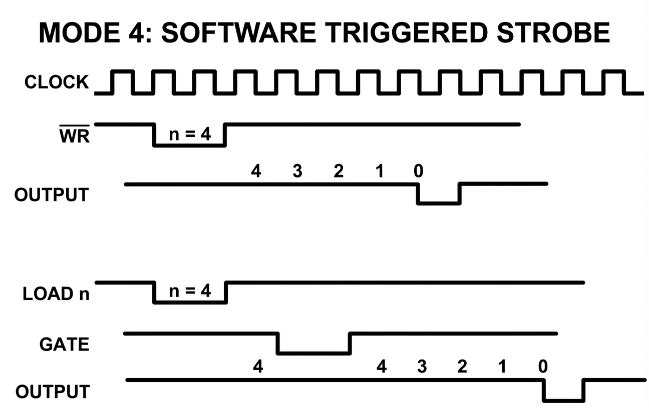
Figure 7: Timer Mode 4 - Software Triggered Strobe Timing
Mode 5 — Hardware Triggered Strobe
Summary
Similar to Mode 4, but triggered by a LOW → HIGH transition of GATE. In Mode 5, OUT goes low on a count of 0, then HIGH again on the next clock edge. The counter will continue to count, rolling over from 0 to 0xFFFF, but will not affect the state of the OUT pin until the counter is retriggered by the GATE pin.
Note: The count starts running as soon as Mode 5 is selected - but you’ll note that the CE is not loaded until a GATE trigger. Presumably, the counting element still contains whatever it had in it when the mode was set, but this has not been verified.
Output Behavior
- After mode set: OUT → HIGH
- At terminal count: OUT → LOW for one clock period
GATE Behavior
- Edge-triggered
- GATE LOW -> HIGH: Trigger. The CR is loaded into the CE on the next clock edge. Counting enabled.
- GATE does not affect OUT,
Reload Behavior
- Writing a new count value during an active count will not affect the current count until either a terminal count or a GATE trigger.
Timing
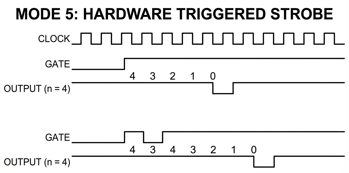
Figure 7: Timer Mode 5 - Hardware Triggered Strobe Timing
Mode Summary Table
| N | Mode | OUT after Mode set | GATE mode | Writing count reloads next clk | Automatic Reload | GATE initiates counting | GATE controls counting |
|---|---|---|---|---|---|---|---|
| 0 | Interrupt on Terminal Count | LOW | Level-triggered | YES | NO | NO | YES |
| 1 | Hardware Retriggerable One Shot | HIGH | Edge-triggered | NO | NO | YES | NO |
| 2 | Rate Generator | HIGH | Both | NO | YES | YES | YES |
| 3 | Square Wave Generator | HIGH | Both | NO | YES | YES | YES |
| 4 | Software Triggered Strobe | HIGH | Level-triggered | YES | NO | NO | YES |
| 5 | Hardware Triggered Strobe | HIGH | Edge-triggered | NO | NO | YES | NO |
Edge Cases
Some interesting edge cases have been observed. Consider the following scenario:
- A timer channel is set to Mode 2 - Rate Generator, RW mode
LSBMSB, and an initial count written, starting the count. - Only the
LSBof a new count is written. - The timer reaches terminal count. What value is loaded into the Counting Element?
- Once the Counting Element has been reloaded, what happens when the
MSBof the new count is then written?
If you have studied the counter channel block diagram, you may be able to figure out what should happen. The \(\text{CR}_m\) and \(\text{CR}_l\) registers are used to hold the programmed initial count, and the CE is reloaded from these registers. In addition, the counter keeps a flip-flop to keep track of the progress of writing a new count, and will write the contents of the CR registers to the CE when the write is complete (depending on mode).
The Intel 8254
The 8254 is an improved model of the 8253 and was used in the IBM AT. It would become the standard timer chip in PC compatible systems for many years.
Changes in the 8254
- Faster clock inputs
- A channel state read-back command
- Resolves the issue with the 8253 where reads and writes to the same channel could not be interleaved without leaving the chip in an undefined state.
- Modified the logic of Mode 3 - Square Wave Generator.
If you wish to emulate the 8254 instead of the 8253, there’s no real problem with doing so.
Emulation Tips
Implementation Priority
- Implement these modes first:
- Mode 3, Square Wave Generator
- Mode 2, Rate Generator
- Mode 0, Interrupt on Terminal Count
- Connect the output of Timer Channel 0 to IRQ0
- Connect the 8255 PPI Port B bit 0 to the GATE of Timer Channel 2
Primary Emulation Resources
- (alldatasheet.com) 8253 Datasheet
- (alldatasheet.com) 8254 Datasheet
- (wiki.osdev.org): Programmable Interval Timer - Mostly describes the 8254
Further Reading
- (wikipedia.org): Intel 8253
- (intel.com @ archive.org): 8254/82C54 Programmable Interval Timer
References
Programmable Peripheral Interface (8255 PPI)
The Intel 8255 PPI is a general-purpose IO chip that provides 24 configurable, bidirectional I/O pins.
The 8255 was used in a number of systems, and even a few mouse controller cards.
The IBM 5150 and 5160 utilize the PPI to receive scancodes from the keyboard interface, read the system’s DIP switches, read motherboard status lines and write control signals.
The PPI is a moderately complex chip with several modes of operation. Perhaps unique to all the support chips you need to emulate, the vast majority of the PPI’s extended capabilities and modes can be completely ignored by a basic PC emulator.
Intel 8237 DMA Controller
The Intel 8237 DMA (Direct Memory Access) Controller enables efficient data transfers between memory and I/O devices without CPU intervention. In the IBM PC, it coordinates data transfer to and from floppy and hard drives, as well as performing DRAM refresh cycles.
Overview
The 8237 provides four independent DMA channels, each capable of transferring data between memory and peripherals. In theory, the 8237 is capable of performing memory-to-memory transfers as well, but its implementation in the IBM PC prevents it from doing so.
IBM PC DMA Configuration
| Channel | Purpose | Device |
|---|---|---|
| 0 | Memory Refresh | DRAM |
| 1 | Unused | - |
| 2 | Floppy Disk | FDC |
| 3 | Hard Disk* | HDC |
Note: Not all hard disk controllers use DMA. Notably, most models of the XTIDE do not.
Hardware Interface
I/O Ports (8237A-5)
| Port | Register | Access |
|---|---|---|
| 0x00 | Channel 0 Address | R/W |
| 0x01 | Channel 0 Count | R/W |
| 0x02 | Channel 1 Address | R/W |
| 0x03 | Channel 1 Count | R/W |
| 0x04 | Channel 2 Address | R/W |
| 0x05 | Channel 2 Count | R/W |
| 0x06 | Channel 3 Address | R/W |
| 0x07 | Channel 3 Count | R/W |
| 0x08 | Status Register | R |
| 0x08 | Command Register | W |
| 0x09 | Request Register | W |
| 0x0A | Mask Register | W |
| 0x0B | Mode Register | W |
| 0x0C | Clear Flip-Flop | W |
| 0x0D | Master Clear | W |
| 0x0E | Clear Mask Register | W |
| 0x0F | Write All Mask Bits | W |
Page Registers
The DMA page registers are not part of the 8237 itself, but are implemented on the motherboard. They are provided here for convenience.
Note: The page register addresses are mapped out of order from their respective channels. Take note of the assignments.
- 0x81: Channel 2 Page Register (Address bits 16-19)
- 0x82: Channel 3 Page Register (Address bits 16-19)
- 0x83: Channel 1 Page Register (Address bits 16-19)
The IBM AT added a page register for Channel 0, but this is not implemented on the PC/XT:
- 0x87: Channel 0 Page (bits 16-19)
DIP switches
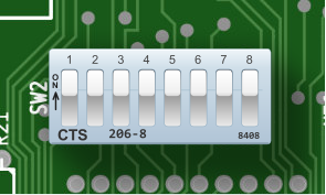
DIP Switch #2 on the IBM 5150
Dual In-line Package (DIP) switches are small electrical components designed to enable a user to configure the operation of a device. DIP switches have an indicated ON position printed on the switch package. In this manner some switches can be turned ON and others turned OFF. DIP switches are not often marked with their effects - typically you would need to consult a manual to determine how they should be set.
Although convenient for device designers to implement, they are somewhat inconvenient for users in that they require a small tool to physically set. On the PC, accessing the DIP switches requires removing the case cover and navigating through any cabling and expansion cards that may be in the way.
The IBM 5150 has two configuration DIP switches. The first one, SW1, is concerned with configuring the amount of memory installed in the system. The second set of DIP switches, SW2, is used to indicate what hardware is installed in the system.
The IBM 5160 XT BIOS added auto-discovery of the amount of memory installed in the system, and so SW1 was removed. The operation of SW2 on the XT is otherwise similar.
Some expansion cards have DIP switches, which are sometimes accessible from the outside of the case through a cut-out in the IO bracket. The IBM EGA card is one such example.
Reading DIP Switches
One gotcha when reading the DIP switches on the PC is that they will read logically inverted from what you may intuit from their physical state. If a DIP switch is set to ON, it will read as a logical 0. If a switch is set to OFF, it will read as a logical 1.
A small schematic will help explain why:
When a switch is OFF, it is electrically open. Pull-up resistors connected to the output side of the switches make them read as logically 1. When a switch is ON, it is electrically closed. The other ends of the switches are connected to ground, and so current flows through the switch and the output side of the switch reads as logically 0.
This was a common way to implement a DIP switch as a connection to ground is a lot easier to find on a PCB than a connection to VCC.
The IBM PC/XT Keyboard Interface
The XT keyboard interface, as it will be referred to from now on, is one of the most frequently misunderstood systems on the IBM PC, confusing both emulator authors and retro-programmers alike. It is easy to write a program that uses the keyboard in a way that works fine on an AT (or in DosBox), but fails on a more accurate XT emulator or real XT system. This is due to some peculiarities of the XT interface, which will be explained here.
The Host Keyboard Interface
The low-level, host-facing interface to the keyboard is implemented via the 8255 PPI. The keyboard is controlled via two bits on Port B, 61h, and the scancodes themselves are read out of Port A, 60h. These particular ports became somewhat standard, and so are often implemented on systems which do not even have an 8255 at all.
| Bits | Name | Description |
|---|---|---|
| 0:5 | Other functions | Other functions - see PPI section |
| 6 | PB6 | 0: Pull keyboard clock line LOW 1: Allow keyboard to drive clock |
| 7 | PB7 | 0: Normal operation 1: Clear KSR + Clear IRQ1 [5150 only: Present SW1 settings to port A] |
The Hardware Keyboard Interface
PB6 is typically used to reset the keyboard. It is wired up to a driver that will connect the keyboard clock line to ground. The control pin of the driver is active-low, which is why setting PB6 to 0 will perform this function, and setting PB6 to 1 allows the keyboard to operate normally.
Here is a simplified schematic:
See the Model F section for more specific details, but if the keyboard clock line is held low for 20ms the keyboard will perform a reset/self-test. The BIOS sometimes does this, but applications usually do not.
The keyboard interface is a typical two-wire serial connection with a clock and a data line. Both of these are pulled high, with either the PC or the keyboard able to drive the lines low. The PC drives the lines low with dedicated drivers; the keyboard takes advantage of the open-collector outputs of its 8048 microcontroller.
This scheme allows simple hardware flow control - when the PC has the clock or data line pulled low, the keyboard cannot send data. The keyboard’s microcontroller can detect when the PC has either line held low, and knows to wait as the PC must either be busy, or requesting a reset. Keys pressed while the data line is held low by the PC will be stored in the keyboard’s internal FIFO until they can be sent. If this FIFO is full, then any additional keystrokes will be lost.
Each scancode is sent as a series of 9 bits. A rising edge of the keyboard clock line triggers the PC to sample the data line, shifting the resulting bit into a 74LS322 shift register, U24. The first bit, called a start bit, is always 1. This is used to good effect - when the Qh output of U24 goes high, this triggers various circuitry that clamps down on the keyboard data line, pulling it low after an additional clock. At this point, the shift register contains the entire 8-bit scancode, which can then be read out of PPI Port A.
Bits are sent over the wire from least-significant (bit 0 of scancode) to most-significant. Here is a logic analyzer capture of the ‘G’ key being pressed (scancode 0x22):
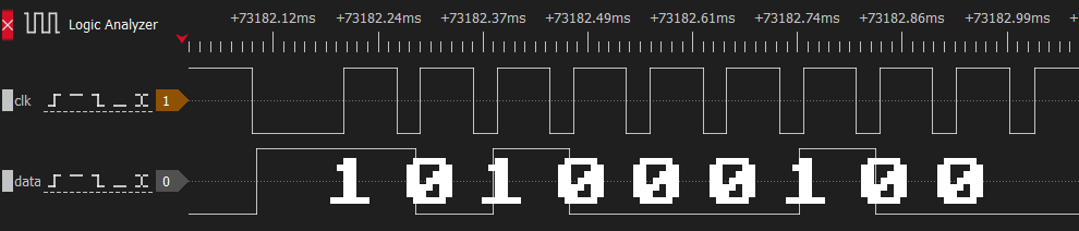
Keyboard scancode 0x22 timing trace (Click to zoom)
Here is a simplified schematic:
Note that a complete scancode being received directly triggers IRQ1, and only writing 1 to PB7 will lower IRQ1 again.
Setting PB7 to 1 does several things:
- It clears the contents of the keyboard shift register U24, making its
Qhoutput low for at least the next 8 clocks. - It disables the parallel outputs of the keyboard shift register U24, making it impossible to read a scancode.
- It resets the flip-flop controlling IRQ1 and the keyboard data line. This forces IRQ1 low, and allows the keyboard to drive the data line.
Therefore, to read the keyboard, software must set PB7 to 1 and then reset it back to 0 after each scancode is read.
Floppy Disk Concepts
If you are already familiar with floppy disks, their operation and organization, skip ahead to the floppy data encoding section.
The floppy disk was the most common form of removable, rewritable storage on the IBM PC. Even when physical distribution of commercial software had moved to the CD-ROM, users still found the floppy disk useful day-to-day for moving files between systems. The main advantage of the floppy disk was its sheer ubiquity — nearly every PC had a floppy drive.
The floppy disk gets its name from its flexibility. If held only by one corner, the disk would easily flex or ‘flop’ when moved.
The floppy disk was originally invented by IBM, which coined the term diskette to refer to their 8“ floppy disks, sometime around the time the IBM 3740 was introduced; however, floppy disks had already been in use for several years by then. The name diskette was frequently seen on floppy disk retail packaging, but colloquially, most people just called them floppies.
A floppy drive was technically an optional add-on for the original PC, but the near total absence of software titles available for the PC on cassette made at least one floppy drive a mandatory purchase.
Floppy disks have existed in numerous forms over the entire history of computing, but the original format used on the PC was the 5.25“ diskette.
| Size | Approx. era | Formatted capacities | Notes |
|---|---|---|---|
| 8“ | 1970s | about 80KiB to 1200KiB | The original commercial floppy format. Used by IBM and early CP/M systems. |
| 5.25“ | late 1970s-1980s | about 90KiB to 1200KiB | The dominant early microcomputer format and the original IBM PC diskette size. |
| 3.5“ | mid-1980s-1990s | 720KiB, 1440KiB, and 2880KiB | A smaller rigid-shell format that gradually replaced 5.25-inch media on PCs. |
| 3“ | mid-1980s | about 180KiB per side to 720KiB | A less common format used mainly by Amstrad and a few other systems. |
| 2“ | 1989 | 720KiB | FujiFilm LT-1 miniature floppy. Used only on the Zenith MinisPort laptop |
Basic Floppy Operation
A floppy disk is a ferromagnetic medium upon which data can be stored by magnetizing the medium in specific patterns. Data is read from and written to the disk via magnetic heads located within a floppy disk drive. A floppy disk drive stores data on a floppy disk in a series of concentric rings called tracks. The magnetic heads travel on a linear carriage controlled by a stepper motor which positions the heads above a specific track to be read or written.
The 5.25“ Diskette
A 5.25“ floppy disk consists of a vinyl jacket covering a circular disc of biaxially oriented polyethylene terephthalate, more commonly known by its brand name, Mylar. A polymeric coating containing carefully milled ferric oxide powder was applied to the surface of this disc, which could then be deliberately magnetized to store specially-encoded data. This inner disc is sometimes referred to as the cookie (or biscuit, if you are from the UK).
The vinyl jacket of a floppy disk has several cutouts. A central hole exposes the inner rim of the Mylar disc which is clamped against the floppy drive spindle when a disk is inserted into a drive and the drive door (sometimes just a lever) is closed. The drive’s spindle motor could then rotate the cookie within the stationary jacket, typically around 300RPM.
A pill-shaped cutout called the data window exposes the usable region of the cookie on both sides, accommodating the full linear travel of the drives’ magnetic heads.
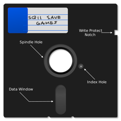
A 5.25" Floppy Disk (Click to zoom)
Near the central spindle, a circular cutout in the jacket allows a photosensor to detect light through a small hole in the Mylar disc called the index hole. When this photosensor — called the index sensor — detects light through the index hole, the drive generates an index pulse. The floppy controller uses the index pulse to know where to start initializing or formatting a track of data. Once a track has been fully written, the index sensor only serves as a useful operational timeout — any disk operation typically must complete within two revolutions of the disk or two index pulses. Not all computer systems utilized an index sensor, with the Apple II the most famous of systems that did not.
The write-protect notch is a rectangular cutout on the right side of the floppy disk that permits data to be written to the floppy disk. A small sticker could be folded over the side of the floppy disk to cover this notch, which would then prevent the host computer from writing data to the disk.
Note
The effect of a write-protect sticker is reversed on 5.25“ disks from the logic used by earlier 8“ disks — on an 8“ disk, you apply a sticker to make the disk writable! This change may have been driven by the increasing importance of commercial software distribution on floppy, allowing manufacturers to produce “notchless” disks that couldn’t be easily overwritten.
The inside of the jacket contains a dust-collecting liner which served the essential function of keeping the inner cookie clean. This part of the floppy may be considered consumable; over time only so much dust can be captured and larger, grittier particles trapped in the liner may even cause damage. Therefore, storing floppy disks in closed, dust-free containers was well-advised.
5.25“ floppy disks were somewhat fragile. They were susceptible to damage from improper handling such as creasing or bending, or directly touching the magnetic coating visible through the data window. Exposure to magnets could damage or erase the data stored on the floppy. That said, if treated with care, the floppy disk was a fairly reliable storage medium.
Over time, floppy disks have faced new challenges. Heat and humidity in long-term storage can lead to the oxide coating flaking off, or mold growth on the cookie which can contaminate the inner lining. Even so, if stored carefully, many floppy disks can still be read a half-century later.
The original floppy diskette was 8“. When the 5.25“ disk was introduced, its smaller size required it to be distinguished from the standard 8“ floppy, and so 5.25“ diskettes were sometimes called minifloppies. Seeing the term minifloppy is a good sign you are reading an older reference.
Single and Double Sided Floppies
The oldest floppy drives were single-sided — they possessed a single magnetic head to read and write data, which was done from the bottom side of the floppy if inserting it label-side up. Single-sided disks could sometimes be flipped over to use the other side, much as you might flip over a vinyl record. These so-called flippy disks could be easily identified by the presence of two index hole cutouts — and sometimes two write-protect notches.
A double-sided floppy drive has two magnetic heads, which clamp together to press against opposite sides of the cookie. You can see an image of a double-sided drive’s magnetic heads below. Head 0, which accesses side 0, is located on the bottom, with side 1 accessed from the top.
The top head is usually on some sort of actuator, where it can be lowered onto the disk surface to clamp the cookie between both heads. This clamping action is called head loading. In a single-sided drive, a foam pad typically provides the clamping force in the absence of an opposing head.
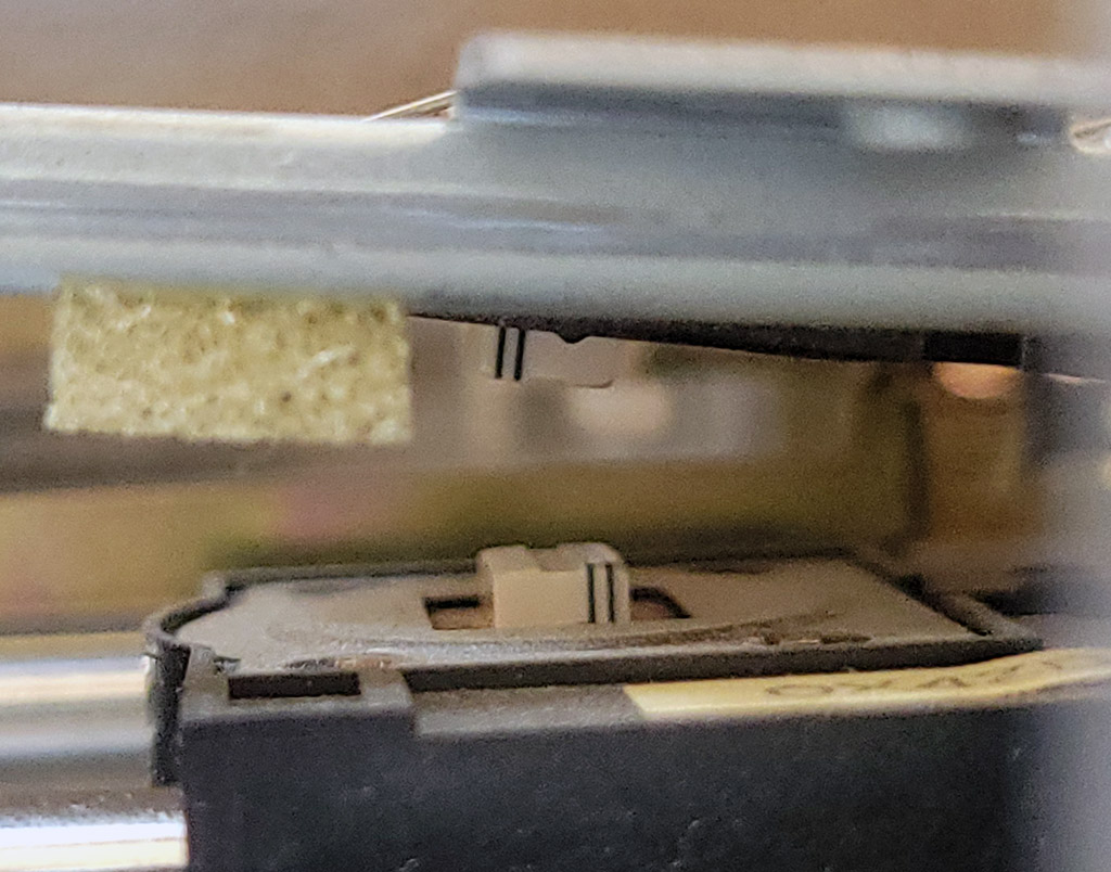
A double-sided floppy drive's magnetic heads
5.25“ Floppy Capacities
5.25“ floppy disks on the IBM PC were available in the following capacities:
| Formatted size | Sides | Tracks | Sectors per track | Notes |
|---|---|---|---|---|
| 160KiB | 1 | 40 | 8 | Original IBM PC single-sided disk |
| 180KiB | 1 | 40 | 9 | Single-sided format with one additional sector per track |
| 320KiB | 2 | 40 | 8 | Double-sided version of the original PC layout |
| 360KiB | 2 | 40 | 9 | Standard double-sided double-density PC format |
| 720KiB | 2 | 80 | 9 | 80-track ‘quad-density’ format, less common on PC |
| 1200KiB | 2 | 80 | 15 | High-density format introduced with the IBM PC AT |
High Density 5.25“ Drive Quirks
One way high-density 5.25“ disk drives increased capacity was by doubling the number of tracks written to high-density 5.25“ diskettes. To do so, the size of the magnetic head itself was made thinner. This can create issues when writing data to double-density diskettes that are then read in a double-density drive with a wider head.
Many high-density 5.25“ drives increase the rotational rate of the cookie to 360RPM, although this can often be controlled by a jumper on the drive. Leaving this setting at 360RPM can cause inaccurate flux timing readings when making flux-level images of double-density diskettes. This can be corrected after the fact, but is not ideal as it can interfere with proper imaging of some copy protection techniques. It is best to image double-density floppy disks in a double-density drive, or at least a high-density drive with the 300RPM mode selected.
The 3.5“ Diskette
The 3.5“ floppy disk was an improvement over the 5.25“ floppy in capacity, durability, and convenience. The 3.5“ floppy disk employed a rigid plastic shell and a metal, spring-loaded shutter to protect the cookie from dust and contact with fingers. A rectangular hole — which could be covered by an integrated plastic slider — controlled whether the disk could be written to or not, meaning awkward stickers were no longer required. When the hole was unobstructed by the slider, the disk was write-protected.

A 3.5" Floppy Disk (Click to zoom)
Later high-density variations of the 3.5“ floppy could be identified by a second hole on the opposite side from the write-protect hole. This allowed the drive to recognize the disk as high density. In addition, a “HD” logo was usually printed on or molded into the plastic shell.
3.5“ diskettes are sometimes referred to as microfloppies.
Note
In more recent years, a contentious debate can occasionally arise over whether the hard-shelled 3.5“ disks were referred to as “floppy disks” — primarily due to their distinct lack of being floppy. The term “floppy disk” generally applied to 3.5“ disks as well in English-speaking countries with the exception of South Africa, where 3.5“ disks were routinely called “stiffy disks”1.
In other countries, other terminology may have been common, but most computer users would have been familiar with the term “floppy disk” in reference to 3.5“ diskettes due to the predominance of US and UK-based media.
3.5“ Floppy Capacities
3.5“ floppy disks on the IBM PC were available in the following capacities:
| Formatted size | Sides | Tracks | Sectors per track | Notes |
|---|---|---|---|---|
| 720KiB | 2 | 80 | 9 | Double-density |
| 1440KiB | 2 | 80 | 18 | High-density: the most common 3.5“ format, but not supported by the original PC |
| 2880KiB | 2 | 80 | 36 | Extra-high density (not common) |
Magnetic Encoding
A floppy disk, like any digital medium, ultimately stores 0s and 1s. A floppy disk encodes binary bits by means of changing magnetic flux.
The Mylar cookie of a floppy disk has a polymeric coating applied to it containing very fine, ferromagnetic particles. On a blank, unformatted disk, these particles are not magnetized in any specific direction. To write data to a floppy disk, the drive magnetizes these particles in specific patterns along concentric rings called tracks.
It might help to visualize the ferromagnetic coating as if it were a number of very small bar magnets with a north and south pole. Data is encoded by alternating the magnetic polarization along a single track as the disk rotates beneath the write head. This is called longitudinal recording.
Note
Later 2880KiB — or “Extra-high density” — floppy drives utilized perpendicular recording, which will not be discussed here.
The ferromagnetic coating is magnetized by the drive’s magnetic write head. A photograph of such a head can be seen below.
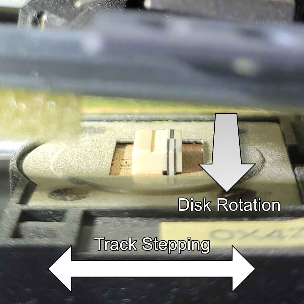
The floppy disk write head in a TEAC FD-55BR disk drive
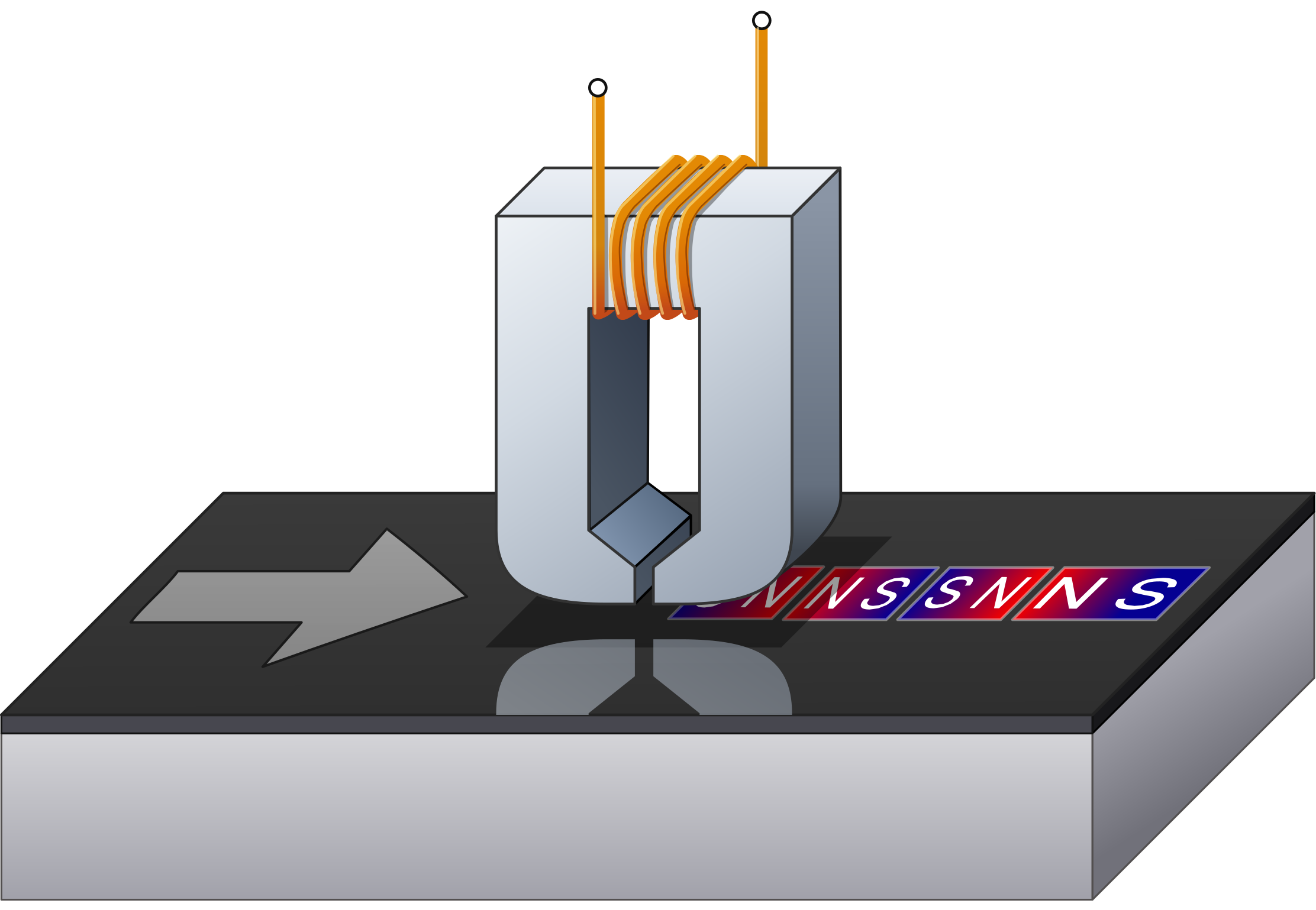
A floppy disk write head
By periodically changing the magnetic orientation, small regions where the polarity flips are also created — these regions are called flux reversals or flux transitions.

A flux transition (representational, not to scale — click to zoom)
When reading a floppy disk, it is these transitions that the drive detects, via Faraday’s Law of Induction. The change in the magnetic field induces a voltage in the coil attached to the read head, creating an electrical signal that can be amplified and turned into a read pulse. These read pulses are sent to a floppy controller, which uses the time between each pulse to recreate the actual bits encoded on the disk.
Data Encoding
The actual bits stored on a floppy disk represent an encoded form of the data written to the disk. Earlier 8“ floppy disks typically used frequency modulation (FM) encoding, whereas most floppy disks for the PC utilize modified frequency modulation (MFM) encoding.
Although FM mode was seldom used, the IBM PC floppy controller could be operated in both FM and MFM modes. The controller would need to be set to the correct mode to successfully read back data originally written with that mode.
The purpose of both encoding schemes is to add clock bits that provide timing information, a technique known as clock recovery.
A requirement for successful clock recovery from the encoded bit stream is ensuring that 1 bits are regularly encoded. This in turn ensures that regular flux transitions are written to the disk. The absence of a flux transition over too long a period risks creating an unstable condition where data cannot be reliably read. As a general rule, no more than three consecutive 0 bits are allowed in the encoded bitstream written to a floppy disk track.
The next chapter, Floppy Data Encoding, covers this subject in more detail.
Density
Density in terms of floppy disks refers to how tightly and efficiently data can be encoded onto a track. Initially this was a combination of both encoding methods and packing flux transitions more tightly together.
All standard floppy disk formats used on an IBM PC use MFM encoding. As this was a space savings improvement over the original FM encoding, this led to the terminology of the double-density diskette often seen on retail packaging and diskette labels. If you were ever curious if there was a “single-density” diskette — these were actually referred to as standard density, but were never used on the PC.
PC floppy disk encoding never moved beyond MFM. Therefore, when high-density and extra-high-density disks emerged, this extra density was simply the result of packing flux transitions more tightly together. This usually necessitated more advanced formulations of ferromagnetic coatings, using more exotic or specially-doped oxides.
Rotation
If viewed from the top, a floppy disk drive rotates the cookie in a clockwise direction, and therefore data is written to the cookie counter-clockwise. When viewed from beneath the drive (from the perspective of head 0), the cookie rotates in a counter-clockwise direction, and therefore data is written clockwise. This rotation is often reflected by disk visualization software.
Most floppy drives on the PC rotate the cookie at 300RPM except for 5.25“ high-density disk drives, which often rotate the cookie at 360RPM.
Note
Some 3.5“ drives — mostly used on non-IBM-PC compatible systems — could rotate at 360RPM, or even at variable RPM depending on which track was being read. These will not be discussed further in this book.
Floppy Disk Organization and Addressing
A floppy disk stores concentric rings of data called tracks. Tracks are identified by a 0-based index, starting at the outer extent of the drive head’s travel (closest to the edge of the disk), counting upwards as the tracks proceed inwards toward the spindle hole. This index is called the cylinder number. A track can be uniquely identified by combining the cylinder number with a specific head, indicating which side of the floppy the track is on.
Tip
The distinction between tracks and cylinders may be somewhat confusing. Think of it as a coordinate system where a track is a combination of cylinder and head — the cylinder specifies how far from the outer edge of the data the drive head should be positioned, and the head determines on which side of the disk the track is located. On a double-sided disk, a cylinder can therefore refer to two unique tracks, one on each side of the disk. On a single-sided disk, the concepts of track and cylinder are fundamentally equivalent.
A floppy drive selects a specific cylinder to operate on by physically moving the magnetic heads until they are over the cylinder. Since the carriage the magnetic heads are on is actuated by a stepper motor, the process of moving from one cylinder to the next is called stepping.
Most PC floppy drives contain a special sensor that can indicate when the magnetic head is positioned at the outermost cylinder. This is called the track 0 sensor. If the position of the magnetic head ever becomes indeterminate, the drive can be recalibrated by seeking to track 0.
Each track contains one or more sectors. Each sector is identified by a sector ID consisting of the cylinder number, head number, sector number, and a sector size specifier. Sector numbers typically begin with 1 on each track by convention, but nothing actually guarantees this.
The combination of cylinder, head, and sector number can uniquely identify a sector on a normally formatted floppy disk. This is sometimes referred to as CHS addressing, which you may also see referenced in the context of early hard drives.
Sectors are aligned on each track by synchronizing to the index pulse created by a photodiode that detects light shining through the physical index hole. With each sector on each track aligned, a floppy disk resembles something like pie slices. Individual sectors are separated by small areas of padding called sector gaps.
Floppy disks are often visualized using diagrams with an exaggerated inner diameter with the index position at the right side, like the one below.
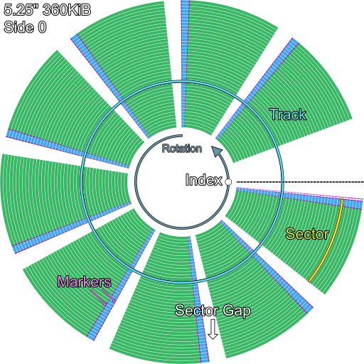
A typical sector layout on a 5.25" 360KiB floppy disk, as seen from head 0 (not to scale)
If one could see the actual track layout on a 5.25“ disk, it would be condensed into the region visible through the data window and accessible along the full travel of the floppy drive’s head carriage. The following diagram attempts to reproduce such an image:
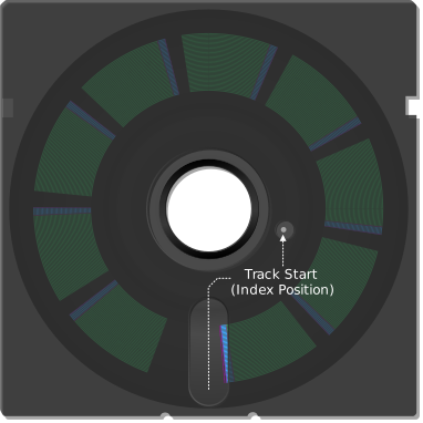
A typical sector layout on a 5.25" 360KiB floppy disk, as seen from head 1
The specification of how data is organized on any given track of a floppy disk is called its track format.
The track format of IBM floppy disks is sometimes referred to as System 34 format, in reference to the IBM System/34, which utilized this format before the PC.
The process of writing out a standard format consisting of a prescribed number of sectors is called formatting. This operation can be performed by a floppy controller with a special formatting command on a per-track basis, but most users will be familiar with formatting an entire disk at a time using a utility such as MS-DOS’s FORMAT.COM.
Sectors: Soft vs Hard
All floppy disks for the PC are soft-sectored. You may see this description as you read various references and wonder what it means. Some earlier 8“ floppy disks were hard-sectored in that they had physical holes punched into the cookie that delineated sector boundaries on the disk. These holes were placed on a radial path aligned with the index hole and so could be read via the same photosensor.
Sectors may be placed anywhere on a PC-formatted floppy disk, thus we can say they are the opposite of hard-sectored: soft-sectored.
Standard PC Floppy Disk Specifications
| 5.25" | 3.5" | |||||||
|---|---|---|---|---|---|---|---|---|
| Standard Capacity | 160KiB | 180KiB | 320KiB | 360KiB | 1200KiB | 720KiB | 1440KiB | 2880KiB |
| Physical Dimensions | 5.25" | 5.25" | 5.25" | 5.25" | 5.25" | 3.5" | 3.5" | 3.5" |
| Default Encoding | MFM | MFM | MFM | MFM | MFM | MFM | MFM | MFM |
| Density | DD | DD | DD | DD | HD | DD | HD | ED |
| Cylinders | 40 | 40 | 40 | 40 | 80 | 80 | 80 | 80 |
| Heads | 1 | 1 | 2 | 2 | 2 | 2 | 2 | 2 |
| Tracks | 40 | 40 | 80 | 80 | 160 | 160 | 160 | 160 |
| Sector Offset | 1 | 1 | 1 | 1 | 1 | 1 | 1 | 1 |
| Sectors Per Track | 8 | 9 | 8 | 9 | 15 | 9 | 18 | 36 |
| Total Sectors | 320 | 360 | 640 | 720 | 2400 | 1440 | 2880 | 5760 |
| RPM | 300 | 300 | 300 | 300 | 360 | 300 | 300 | 300 |
| Revolution Time | 200ms | 200ms | 200ms | 200ms | 166ms | 200ms | 200ms | 200ms |
| Raw bit rate (kbps) | 500 | 500 | 500 | 500 | 1000 | 500 | 1000 | 2000 |
| MFM Data rate (kbps) | 250 | 250 | 250 | 250 | 500 | 250 | 500 | 1000 |
| kb/track | 50 | 50 | 50 | 50 | 83.3 | 50 | 100 | 200 |
| Bitcell/track | 100000 | 100000 | 100000 | 100000 | 166666 | 100000 | 200000 | 400000 |
| TPI | 48 | 48 | 48 | 48 | 96 | 135 | 135 | 135 |
Floppy Data Encoding
If you are not already familiar with floppy disks, their operation and organization, you may wish to review the prior section on floppy disk concepts.
Before data can be written to a floppy disk, it must first be encoded using a scheme to make the data compatible with storage via timed flux transitions.
An encoding scheme has the primary job of making clock recovery possible, since data transfer to and from a floppy drive is a serial stream with no independent clock line. By inserting clock bits, an encoding scheme can allow the controller to synchronize with the rate data is being streamed from any given floppy drive while accounting for factors such as slightly too fast or slightly too slow spindle motors, RPM wobble, or basic signal jitter.
A variety of encoding schemes have been used on floppy disks over the years, but only one — MFM — is primarily relevant on PC.
| Encoding | Name | Typical use | Notes |
|---|---|---|---|
| FM | Frequency modulation | Early 8“ floppies and occasionally elsewhere | Simple, but inefficient |
| MFM | Modified frequency modulation | IBM PC-compatible floppy formats | The dominant PC floppy encoding for “double density” diskettes, more efficient than FM |
| GCR | Group coded recording | Apple, Commodore, and other non-PC floppy systems | Encodes groups of data bits into code words. |
| MMFM | Modified modified frequency modulation | Some non-PC or specialized floppy formats | A less common MFM variant that further improves efficiency |
Almost all floppy disks written for the IBM PC use primarily MFM encoding for user-accessible data.
Note
FM-encoded sectors do regularly appear on commercially duplicated software titles, usually on the very last track of a floppy. These are called duplication marks. They often contain metadata about the publisher, duplication parameters, and sometimes even the copy-protection scheme employed. It is not critical that your emulator be able to read them, and only certain disk images can encode them, anyway.
FM Encoding
FM encoding is conceptually very simple. 1 bits are inserted between each data bit of the data stream to be encoded. An FM-encoded data stream will begin with an initial 1 clock bit.
If we begin with the bit sequence 1100_0101, after inserting clock bits, we are left with the sequence 1111_1010_1011_1011.
The clock and data bits interleave like so:
| Source | 0 | 1 | 2 | 3 | 4 | 5 | 6 | 7 | 8 | 9 | 10 | 11 | 12 | 13 | 14 | 15 |
|---|---|---|---|---|---|---|---|---|---|---|---|---|---|---|---|---|
| Original data bits | 1 | 1 | 0 | 0 | 0 | 1 | 0 | 1 | ||||||||
| Clock bits | 1 | 1 | 1 | 1 | 1 | 1 | 1 | 1 | ||||||||
| FM-encoded byte | 1 | 1 | 1 | 1 | 1 | 0 | 1 | 0 | 1 | 0 | 1 | 1 | 1 | 0 | 1 | 1 |
A trivial encoding table can be constructed:
| Data Bit | Output FM Sequence |
|---|---|
0 | 10 |
1 | 11 |
Since there are only two possible output sequences, FM-encoded data is magnetically encoded with two discrete flux transition periods, which we will call short and long transitions. These periods refer to the time between a pair of flux transitions.
| Period Type | Encodes | Period Length |
|---|---|---|
| Short | 1 | 4 microseconds at a 250kHz FM write clock |
| Long | 01 | 8 microseconds at a 250kHz FM write clock |
Note that FM encoded data becomes twice as long as the source data it encodes. For this reason other, more efficient encoding schemes became more popular.
MFM Encoding
MFM encoding improves on FM by only inserting clock bits where they are needed for clock recovery. A clock bit is written before a 0 data bit only when the previous data bit was also 0; all other clock positions are left empty, represented as 0 in the encoded cell stream. Since encoding any particular bit sequence into MFM requires knowledge of the previous bit in the stream, we can say that MFM is a stateful encoding scheme.
The mathematical representation of MFM encoding can be written as:
$$ (x, y, z) \to (x, \overline{x \vee y}, y, \overline{y \vee z}, z, \ldots) $$
Some sort of data leader or sync region may be needed to initialize a MFM data stream since there will always be a first bit in any stream, which will by definition not have a valid previous bit.
If we begin with the same bit sequence as before, 1100_0101, and assume that the previous data bit was 0, MFM encoding gives us the sequence 0101_0010_1001_0001.
The clock and data cells interleave like so:
| Source | 0 | 1 | 2 | 3 | 4 | 5 | 6 | 7 | 8 | 9 | 10 | 11 | 12 | 13 | 14 | 15 |
|---|---|---|---|---|---|---|---|---|---|---|---|---|---|---|---|---|
| Original data bits | 1 | 1 | 0 | 0 | 0 | 1 | 0 | 1 | ||||||||
| Clock cells | 0 | 0 | 0 | 1 | 1 | 0 | 0 | 0 | ||||||||
| MFM-encoded byte | 0 | 1 | 0 | 1 | 0 | 0 | 1 | 0 | 1 | 0 | 0 | 1 | 0 | 0 | 0 | 1 |
When encoding a stream of bits into MFM one has to account for the previous data bit. In the table below, - means that no clock bit is inserted:
| Current Data Bit | Previous Data Bit | Inserted Clock Bit | Output MFM Sequence |
|---|---|---|---|
0 | 0 | 1 | 10 |
0 | 1 | - | 00 |
1 | 0 | - | 01 |
1 | 1 | - | 01 |
Although MFM still doubles the length of the encoded bitstream, it allows for more efficient representation as time between flux transitions, reducing the total number of transitions required. MFM is twice as efficient as FM as a result.
MFM-encoded data is magnetically encoded with three discrete flux transition periods. These periods refer to the time between a pair of flux transitions.
| Period Type | Encodes | Period Length |
|---|---|---|
| Short | 10 | 4 microseconds at a 500kHz MFM write clock |
| Medium | 100 | 6 microseconds at a 500kHz MFM write clock |
| Long | 1000 | 8 microseconds at a 500kHz MFM write clock |
Note
You may see references begin the bitwise expansion of a flux transition time with either a
0or1, putting the1bit on either end. Either notation is functionally equivalent, since the period between flux transitions essentially defines the number of0’s between two1’s.
Marker Sequences
FM and MFM encoding specify standard rules by which data is encoded into clock and data bits, and subsequently into flux transitions. Breaking those rules would naturally produce an illegal stream, which we might refer to as an MFM error in the case of MFM encoding.
There are however circumstances where an invalid MFM sequence can be allowed. One such use case is for defining track markers. A track marker is a specially encoded run of data that uses a unique, detectable pattern of clock bits that essentially allows it to stand out from normally-encoded data. A sort of out-of-band signal, if you will.
For example, an MFM sector ID address marker (IDAM) contains three specially-encoded A1 bytes. Each has the data pattern A1, but uses a clock pattern of 0A instead of the normal MFM clock pattern of 0E. This creates a single, missing 1 bit in the clock signal - enough for a floppy drive controller to identify the sequence as a marker.
| Source | Hex | 0 | 1 | 2 | 3 | 4 | 5 | 6 | 7 | 8 | 9 | 10 | 11 | 12 | 13 | 14 | 15 |
|---|---|---|---|---|---|---|---|---|---|---|---|---|---|---|---|---|---|
| Data cells | A1 |
1 |
0 |
1 |
0 |
0 |
0 |
0 |
1 |
||||||||
| Normal clock cells | 0E |
0 |
0 |
0 |
0 |
1 |
1 |
1 |
0 |
||||||||
| Marker clock cells | 0A |
0 |
0 |
0 |
0 |
1 |
0 | 1 |
0 |
||||||||
| Marker Encoding | 4489 |
0 |
1 |
0 |
0 |
0 |
1 |
0 |
0 |
1 |
0 |
0 | 0 |
1 |
0 |
0 |
1 |
Primary References
- (floppy.cafe) MFM Encoding
The Floppy Disk Controller
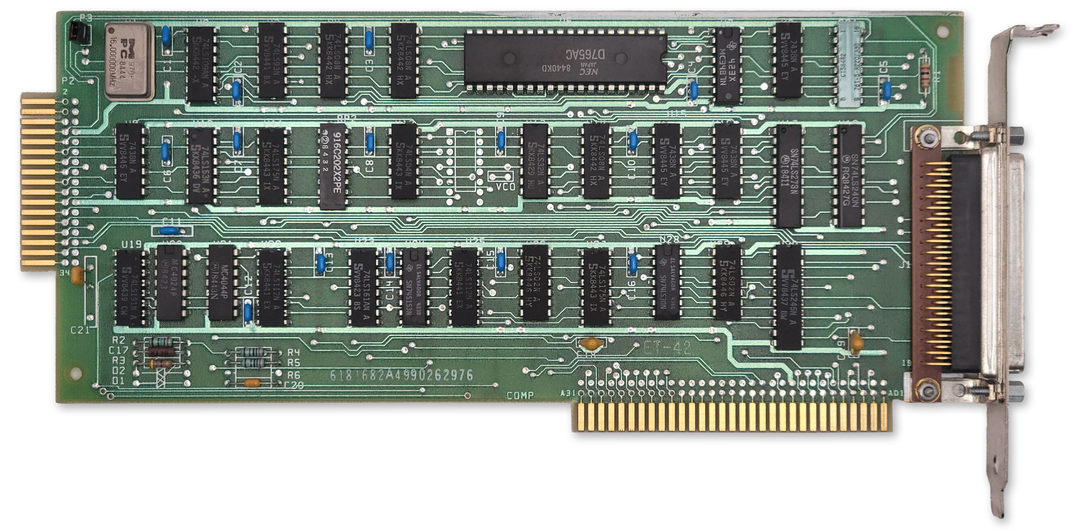
The IBM 5.25" Diskette Drive Adapter
IBM PC/XT systems outfitted with a floppy disk drive had an IBM 5.25“ Diskette Drive Adapter card installed in one of the available expansion slots.
At a Glance
| Item | Description |
|---|---|
| Controller IC | NEC µPD765A or Intel P8272A |
| Adapter clock | 16.0MHz crystal; 8MHz controller clock |
| Supported drives | Up to 4 |
| DMA Channel | Channel 2 |
| Interrupt | IRQ6 |
| Primary I/O range | 3F0h-3F7h |
| Secondary I/O range | 370h-377h |
| DOR | 3F2h primary, 372h secondary |
| Main status register | 3F4h primary, 374h secondary |
| Data register | 3F5h primary, 375h secondary |
| Expansion ROM | None |
Controller Overview
The IBM floppy drive controller, as we’ll refer to it here, was a collection of 74-series logic chips and a 16.0MHz clock crystal supporting the “brain” of the card, a NEC µPD765A (NEC 765) floppy drive controller chip (or the more-or-less identical Intel P8272A).
Note
Microscope photography of the Intel P8272A has revealed the numbers ‘765’ are present on the die, implying Intel licensed NEC’s design and the controllers can be considered basically identical.
The IBM floppy controller could support up to four floppy disk drives, although configurations of more than two were uncommon. Drives 0-3 would be assigned the drive letters A-D up until MS-DOS 5.0, whereupon DOS started to reserve drive letter C for hard disks. It might feel a bit cursed to have a floppy disk as drive C, but if you did indeed have three drives connected and an earlier version of MS-DOS, that’s what you’d end up with.
The NEC 765 takes an 8MHz clock, divided once from the card’s 16MHz crystal. It has a maximum data rate of 250kbps, limiting it to support of double-density diskettes only.
The 765 doesn’t perform every function needed by a floppy controller. Notably, the controller’s voltage-controlled oscillator (VCO), a crucial part of the controller’s phase-locked-loop (PLL) is external to the 765, although the 765 has pins for interacting with it. Also external to the 765 is the data separator circuitry.
Operation
On the IBM PC/XT, the floppy drive controller is operated by the BIOS in DMA mode exclusively. It is possible to operate the controller in polled-io mode (PIO) in a manual fashion, but there are severe disadvantages to doing so - as was seen on the IBM PCjr which lacked a DMA controller. The lack of DMA prevented such operations as transferring data via the serial ports and floppy disk drive at the same time.
The 765 operates as a state machine with three basic operational phases:
- During the command phase the controller receives bytes from the host that instruct it to perform a specific operation.
- During the execution phase the controller carries out the operation specified in the command phase.
- During the result phase the controller provides status information to the host describing the result of the execution phase.
The 765 is capable of running some operations such as Seek and Recalibrate on multiple drives simultaneously.
The 765 maintains an internal register holding the current cylinder, called the Present Cylinder Number (PCN), for each of the four supported disk drives.
I/O Ports
The IBM Diskette Drive Adapter decodes the following I/O port addresses:
| Primary | Secondary | 765 Port | RW | Description |
|---|---|---|---|---|
3F0h | 370h | n/a | Base Address | |
3F2h | 372h | n/a | W | Digital Output Register |
3F4h | 374h | 0 | R | µPD765A Status Register |
3F5h | 375h | 1 | RW | µPD765A Data Register |
Floppy Controller Cable Pinout
The IBM floppy controller has two connectors, an internal and external connector, each supporting two drives. The external connector will not be discussed here as it was rarely used.
The internal connector is of the edge connector type, and contains 34 contacts. Other floppy controllers may have a 34-pin, double-row male header.
All of the odd pins of the connector — one entire side — consist of ground connections. That leaves the other side with the following pinout:
| Pin | I/O | Purpose |
|---|---|---|
| 2 | Unused | |
| 4 | Unused | |
| 6 | Unused | |
| 8 | Input | |
| 10 | Output | Motor Enable A |
| 12 | Output | Drive Select B |
| 14 | Output | Drive Select A |
| 16 | Output | Motor Enable B |
| 18 | Output | |
| 20 | Output | |
| 22 | Output | |
| 24 | Output | |
| 26 | Input | |
| 28 | Input | |
| 30 | Input | |
| 32 | Output | |
| 34 | Unused |
IBM floppy drive cables famously have a twist that reverses conductors 10—16. This allows every drive used in an IBM PC to be configured as drive 1 (DS1). This means that the drive desired to be the first floppy drive (A) should be at the end of the floppy cable.
Floppy Drive Communication
The electrical interface to a floppy drive is rather simple in concept. The controller manipulates the drive select and motor lines to activate the desired floppy drive and spin its motor up to its operating RPM. While rotating, regular, active-low pulses of the signal occur as the floppy drive’s index sensor detects the index hole. As the drive detects flux transitions, active-low pulses of the signal occur. If the controller wishes to write data, it will assert and then provide the appropriate pulses on the .
The controller specifies which head should be active via the output. If this signal is asserted, then head 1 is specified for all operations.
The controller can detect when the drive is positioned at the outermost track, track 0, via an active-low signal.
The Digital Output Register
The IBM controller card adds a main control register external to the 765, called the Digital Output Register or DOR. The DOR has several functions — it selects a specific drive as the target of operations, it can reset the 765, it can enable or disable interrupts and DMA, and it can turn on and off the attached floppy drive motors.
The DOR is a write-only register implemented with a 74LS273 8-bit register chip.
| Bits | Name | Description |
|---|---|---|
| 0:1 | DR | DR: Selected drive |
| 2 | RESET | Controller reset gate 0: Hold controller in reset 1: Enable controller |
| 3 | DMA | DMA and interrupt request enable 0: Disable DMA/IRQ 1: Enable DMA/IRQ |
| 4 | MOTA | Drive A motor control 0: Motor off 1: Motor on |
| 5 | MOTB | Drive B motor control 0: Motor off 1: Motor on |
| 6 | MOTC | Drive C motor control 0: Motor off 1: Motor on |
| 7 | MOTD | Drive D motor control. 0: Motor off 1: Motor on |
DR: Selected drive
| DR1 | DR0 | Drive |
|---|---|---|
| 0 | 0 | 0 (A) |
| 0 | 1 | 1 (B) |
| 1 | 0 | 2 (C/D) |
| 1 | 1 | 3 (D/E) |
Drive Selection Bits
The two least significant bits (Bits 0—1) of the DOR control which floppy drive is selected.
Important
If a drive’s motor is not on, selecting it in the DOR will do nothing until the motor is turned on.
To avoid confusion, be aware that the DOR is the only drive selection method used by the IBM floppy drive controller. The NEC 765 command set includes fields that select which drive the operation is intended to target. Under IBM’s controller design, these bits do nothing externally — the 765 is not in control of which drive is selected. You can verify this yourself by noting the 765’s unit select pins, 28 and 29, are not connected on the schematic.
Important
Even though the 765 does not control drive selection, a programmer should ensure that the drive selected in the DOR matches the drive number specified in commands. A mismatch in the drive selected in the DOR and command phase can cause incorrect operation of the Seek and Recalibrate commands.
Reset Bit
The DOR’s bit 2 drives the 765’s active-high RST pin (1) via an inverter. When a 1 is written to bit 2, the 765’s RST pin is pulled low, holding the controller in reset.
Note
The IBM floppy controller card ties the 765’s RDY pin (35) high. This causes the 765 to generate an interrupt after coming out of the RESET state after “1-25ms”, according to the datasheet. The controller is reset quite often during normal operation.
The 765 Registers
The 765 contains five status registers in total. The first of these is the main status register (MSR). The MSR is the only status register that may be read at any time. The contents of the other status registers, ST0—ST3, are sent to host during the controller result phase.
The Main Status Register
| Bits | Name | Description |
|---|---|---|
| 0 | D0B | Drive 0 (A) is performing a seek or recalibrate operation |
| 1 | D1B | Drive 1 (B) is performing a seek or recalibrate operation |
| 2 | D2B | Drive 2 (C) is performing a seek or recalibrate operation |
| 3 | D3B | Drive 3 (D) is performing a seek or recalibrate operation |
| 4 | BUSY | Controller is busy |
| 5 | NDMA | Non-DMA execution mode indicator 0: Controller in DMA mode 1: Controller in PIO (Non-DMA mode) |
| 6 | DIO | Data Input/Output Direction 0: Host to controller 1: Controller to host |
| 7 | MRQ | Main Request 0: The controller is not expecting to send or receive data 1: The controller has data to send to the CPU, or is ready to receive the next byte of data |
The BUSY bit
The BUSY bit is set when the controller is executing a command, and is only cleared when the last byte of the result phase has been read by the host CPU. It can be used as a general indication that a new command should not be sent to the CPU.
The DIO bit
The DIO bit controls the direction of transfer to or from the controller. The CPU should only send data to the controller when DIO is 0. When DIO is 1, the controller is not ready to receive data — it expects to have data to send to the CPU.
The MRQ bit
The MRQ bit can be usefully combined with the DIO bit to control data transfer to and from the controller.
| DIO | MRQ | Meaning |
|---|---|---|
| 0 | 0 | FDC is not ready to receive a byte from the CPU. (Busy, reset/disabled, or DMA operation in progress) |
| 0 | 1 | FDC is ready and expecting to receive a command or data byte from the CPU via the data register. |
| 1 | 0 | FDC has data pending, but not yet ready to read. |
| 1 | 1 | FDC has a byte ready for the CPU to read from the data register. Result bytes, sense bytes, or PIO read data. |
Note
This bit may also be labelled as
RQMin technical references.
Status Register 0 (ST0)
| Bits | Name | Description |
|---|---|---|
| 0:1 | US | US: Unit select |
| 2 | HD | Currently active drive head |
| 3 | NR | Drive not ready |
| 4 | EC | Equipment check 0: No fault detected. 1: The target drive reports a fault, or track 0 sensor may be inoperable |
| 5 | SE | Seek end 0: No seek performed. 1: The controller successfully executed a seek or recalibrate operation. This includes commands with an implicit seek. |
| 6:7 | IC | IC: Interrupt code |
US: Unit select
| US1 | US0 | Drive |
|---|---|---|
| 0 | 0 | 0 (A) |
| 0 | 1 | 1 (B) |
| 1 | 0 | 2 (C/D) |
| 1 | 1 | 3 (D/E) |
IC: Interrupt code
| IC1 | IC0 | Meaning |
|---|---|---|
| 0 | 0 | Normal termination |
| 0 | 1 | Abnormal termination The controller encountered an error condition during the execution phase. |
| 1 | 0 | Invalid command |
| 1 | 1 | Polling status change A drive became ready or became not-ready during a drive poll. |
Note
The IBM floppy controller does not connect the typical floppy drive indication line, pin 34. Therefore the NR bit will typically not be set, even if the drive door is open and/or no disk is inserted into the drive. If you emulate this bit anyway, you may receive a “General Failure” error message in DOS when no disk is inserted instead of the expected “Not Ready Reading Drive” error.
Correspondingly, since a drive cannot report not-ready during the execution phase, an IC code of
11bwill not be encountered.
Note
The IBM floppy controller does not accommodate an external fault signal, nor do most PC floppy drives supply one. Therefore the EC field can only report failure of the Track 0 sensor during a Seek or Recalibrate operation.
Status Register 1 (ST1)
| Bits | Name | Description |
|---|---|---|
| 0 | MA | Missing ID address mark. |
| 1 | NW | Not writable 1: A write operation was attempted, but the drive reported the media is write-protected. |
| 2 | ND | No Data 1: A required sector ID was not found during the execution phase. |
| 3 | Unused | Unused, always 0 |
| 4 | OR | Overrun/Timeout 1: The controller was not serviced within the required time window, and the operation has failed. |
| 5 | DE | Data error 1: The controller detected a bad CRC in either the sector address or data fields. |
| 6 | Unused | Unused, always 0 |
| 7 | EN | End of Cylinder 1: The controller attempted to access a sector beyond the last sector on a track. |
The No-Data Bit
The No-Data bit is set under the following conditions:
- The FDC could not find the requested sector during execution of
READ DATA,WRITE DELETED DATAorSCAN - The FDC could not read the ID field during execution of
READ ID - The FDC could not find the starting sector during execution of
READ CYLINDER.
Status Register 2 (ST2)
| Bits | Name | Description |
|---|---|---|
| 0 | MD | Missing Data 1: The FDC could not find a data address mark (DAM) or deleted data address mark (DDAM). |
| 1 | BC | Bad cylinder 1: A sector ID with a C of FF was encountered and not explicitly requested. |
| 2 | SN | Scan Not Satisfied 1: During execution of SCAN, no sector satisfying the scan condition could be located. |
| 3 | SH | Scan Equal Hit 1: The EQUAL condition was satisfied during execution of SCAN. |
| 4 | WC | Wrong cylinder 1: A sector ID was encountered specifying a C that does not match the requested C. |
| 5 | DD | Data Error In Data Field 1: The FDC encountered a bad data field CRC. |
| 6 | CM | Control Mark 1: During READ DATA or SCAN, a deleted data address mark (DDAM) was encountered, ORDuring READ DELETED DATA a normal data address mark (DAM) was encountered. |
| 7 | Unused | Unused |
Status Register 3 (ST3)
| Bits | Name | Description |
|---|---|---|
| 0:1 | US | US: Unit select The state of the 765’s unit select pins. |
| 2 | HD | Head address The side select signal from the floppy drive. |
| 3 | TS | Two-sided signal The two side signal from the floppy drive. |
| 4 | T0 | Track 0 The track 0 signal from the floppy drive. |
| 5 | RY | Drive ready The ready signal from the floppy drive. |
| 6 | WP | Write-protect status 1: The floppy drive reports the media is write-protected. |
| 7 | FT | Fault Signal 1: The floppy drive is in a fault condition. |
US: Unit select
| US1 | US0 | Drive |
|---|---|---|
| 0 | 0 | 0 (A) |
| 0 | 1 | 1 (B) |
| 1 | 0 | 2 (C/D) |
| 1 | 1 | 3 (D/E) |
Important
Remember that on the IBM floppy controller, the 765’s unit select pins are not connected and do not drive selection of floppy drives.
Controller Commands
The 765 supports 15 different commands:
| Code | Command Name | MT | MF | SK |
|---|---|---|---|---|
06h | Read Data | ✔️ | ✔️ | ✔️ |
0Ch | Read Deleted Data | ✔️ | ✔️ | ✔️ |
0Ah | Read ID | 0 | ✔️ | 0 |
02h | Read Track | 0 | ✔️ | ✔️ |
11h | Scan Equal | ✔️ | ✔️ | ✔️ |
19h | Scan Low or Equal | ✔️ | ✔️ | ✔️ |
1Dh | Scan High or Equal | ✔️ | ✔️ | ✔️ |
03h | Specify | 0 | 0 | 0 |
05h | Write Data | ✔️ | ✔️ | 0 |
09h | Write Deleted Data | ✔️ | ✔️ | 0 |
0Fh | Seek | 0 | 0 | 0 |
07h | Recalibrate | 0 | 0 | 0 |
0Dh | Format Track | 0 | ✔️ | 0 |
08h | Sense Interrupt Status | 0 | 0 | 0 |
04h | Sense Drive Status | 0 | 0 | 0 |
Commands consist of 2—9 command bytes, sent during the command phase. The command will then enter the execution phase. When complete (or on error) the command enters the result phase and various status register bytes will be made available to read out from the data register.
The first command code byte 0 is common to all commands and contains the command code as given in the table above, along with operational flags. These flags are not always applicable to each command. The flags applicable to each command are noted in the table above.
Command Code Byte 0
| Bits | Name | Description |
|---|---|---|
| 0:4 | Command | Five-bit command number |
| 5 | SK | Skip deleted data address marks |
| 6 | MF | MFM/FM mode select 1: MFM mode selected. 0: FM mode selected. |
| 7 | MT | Multi-track operation 1: Request multi-track operation 0: Normal operation |
Command Code Byte 1
| Bits | Name | Description |
|---|---|---|
| 0:1 | DR | DR: Drive select |
| 2 | HD | Head select |
| 3:7 | Reserved | Reserved |
DR: Drive select
| US1 | US0 | Drive |
|---|---|---|
| 0 | 0 | 0 (A) |
| 0 | 1 | 1 (B) |
| 1 | 0 | 2 (C/D) |
| 1 | 1 | 3 (D/E) |
Sector Size (N)
Many commands take a parameter N which represents the size of the sector to operate on. N is not the actual sector size, but can be used to calculate it by shifting 128 left by the value of N (ex: 128 << N).
The following values of N are valid:
| Value | Meaning |
|---|---|
| 0 | 128/DTL |
| 1 | 256 |
| 2 | 512 |
| 3 | 1024 |
| 4 | 2048 |
| 5 | 4096 |
| 6 | 8192 |
Note
The largest sector size supported by the 765 is N==6, or 8192 bytes. Some controllers support larger values of N, but this is already impractical as an 8192 byte sector will wrap completely around the track.
An N of 0 is special. This indicates a sector size of 128 bytes, but fewer than 128 bytes can be read from a sector with N == 0 via means of the DTL field.
Data Length (DTL) Field
When reading or writing most sectors with N > 0, the DTL field is not used, and should be set to FFh.
When reading or writing a sector with N == 0, the DTL field is honored, up to a maximum of 128 bytes. The entire sector is still read and written, to either validate the CRC in the case of reading, or to calculate and write the CRC in case of writing. In the write case, the unspecified bytes of the sector are padded with 00h.1
The Read Data Command
The Read Data command is opcode 06h.
The Read Data command searches for the sector ID matching the specified cylinder, head, sector and sector size. The matching sector must have a normal data address mark (DAM).
In DMA mode, it will read successive sectors that have a normal DAM until terminal count. In PIO mode, it will read successive sectors that have a normal DAM until EOT is reached.
If the MT flag is set, once the last sector of side 0 is transferred, the FDC proceeds to repeat the operation on side 1.
The Read Data command behaves as follows depending on the value of the SK flag:
| SK | DAM Type | Sector Read | CM | Result |
|---|---|---|---|---|
| 0 | Normal | Y | 0 | Normal Termination |
| 0 | Deleted | Y | 1 | No Further Sectors Read |
| 1 | Normal | Y | 0 | Normal Termination |
| 1 | Deleted | N | 1 | Sector Skipped |
After the data is transferred, the command enters the result phase.
Status Flags Affected
| Flag | Register | Triggering Event |
|---|---|---|
| WC | ST2 | Value of C mismatch in Sector ID |
| BC | ST2 | Value of C mismatch in Sector ID and C was 0xFF |
| CM | ST2 | A deleted data address mark (DDAM) was encountered |
| ND | ST1 | No matching Sector ID was found |
| MA | ST1 | No sector ID address mark (IDAM) was found within two index pulses |
| DE | ST1 | A bad data field CRC was encountered |
Command Format
| Phase | Byte | Byte |
|---|---|---|
| Command | 0 | Command Code Byte 0 |
| Command | 1 | Command Code Byte 1 |
| Command | 2 | Cylinder |
| Command | 3 | Head |
| Command | 4 | Sector |
| Command | 5 | Sector Size (N) |
| Command | 6 | End of Track |
| Command | 7 | Gap 3 Length |
| Command | 8 | Data Length (DTL) |
| Result | 0 | ST0 |
| Result | 1 | ST1 |
| Result | 2 | ST2 |
| Result | 3 | Cylinder |
| Result | 4 | Head |
| Result | 5 | Sector |
| Result | 6 | Sector Size (N) |
The Read Deleted Data Command
The Read Deleted Data command is opcode 0Ch.
The Read Deleted Data command searches for the sector ID matching the specified cylinder, head, sector and sector size. The matching sector must have a deleted data address mark (DDAM).
In DMA mode, it will read successive sectors that have a DDAM until terminal count. In PIO mode, it will read successive sectors that have a DDAM until EOT is reached.
If the MT flag is set, once the last sector of side 0 is transferred, the FDC proceeds to repeat the operation on side 1.
The Read Deleted Data command behaves as follows depending on the value of the SK flag:
| SK | DAM Type | Sector Read | CM | Result |
|---|---|---|---|---|
| 0 | Normal | Y | 1 | No Further Sectors Read |
| 0 | Deleted | Y | 0 | Normal Termination |
| 1 | Normal | N | 1 | Sector Skipped |
| 1 | Deleted | Y | 0 | Normal Termination |
After the data is transferred, the command enters the result phase.
Status Flags Affected
| Flag | Register | Triggering Event |
|---|---|---|
| WC | ST2 | Value of C mismatch in Sector ID |
| BC | ST2 | Value of C mismatch in Sector ID and C was 0xFF |
| CM | ST2 | A normal data address mark (DAM) was encountered |
| ND | ST1 | No matching Sector ID was found |
| MA | ST1 | No sector ID address mark (IDAM) was found within two index pulses |
| DE | ST1 | A bad data field CRC was encountered |
Command Format
| Phase | Byte | Byte |
|---|---|---|
| Command | 0 | Command Code Byte 0 |
| Command | 1 | Command Code Byte 1 |
| Command | 2 | Cylinder |
| Command | 3 | Head |
| Command | 4 | Sector |
| Command | 5 | Sector Size (N) |
| Command | 6 | End of Track |
| Command | 7 | Gap 3 Length |
| Command | 8 | Data Length (DTL) |
| Result | 0 | ST0 |
| Result | 1 | ST1 |
| Result | 2 | ST2 |
| Result | 3 | Cylinder |
| Result | 4 | Head |
| Result | 5 | Sector |
| Result | 6 | Sector Size (N) |
The Read ID Command
The Read ID command is opcode 0Ah.
The FDC returns the fields of the next Sector ID encountered on the track.
The MT and SK flags are not valid for this command and should be 0.
Status Flags Affected
| Flag | Register | Triggering Event |
|---|---|---|
| MA | ST1 | No sector ID address mark (IDAM) was found within two index pulses |
Command Format
| Phase | Byte | Byte |
|---|---|---|
| Command | 0 | Command Code Byte 0 |
| Command | 1 | Command Code Byte 1 |
| Result | 0 | ST0 |
| Result | 1 | ST1 |
| Result | 2 | ST2 |
| Result | 3 | Cylinder |
| Result | 4 | Head |
| Result | 5 | Sector |
| Result | 6 | Sector Size (N) |
The Read Track Command
The Read Track command is opcode 02h.
Unlike what its name might suggest, Read Track does not actually read a raw track. Instead, it reads all sectors on a track, regardless of ID or CRC validation.
The Read Track command first waits for the index signal. It then returns the data for each sector encountered, in order. The Sector ID of the first sector is checked against the values given to the command for the purposes of setting the ND bit in ST1, but a mismatch is not an error and does not stop command execution.
The MT and SK flags are not valid for this command and should be 0.
Status Flags Affected
| Flag | Register | Triggering Event |
|---|---|---|
| ND | ST1 | Sector ID comparison failed (command continues) |
| DD | ST2 | A bad data field CRC was encountered (command continues) |
| DE | ST1 | A bad field CRC was encountered (command continues) |
Command Format
| Phase | Byte | Byte |
|---|---|---|
| Command | 0 | Command Code Byte 0 |
| Command | 1 | Command Code Byte 1 |
| Result | 0 | ST0 |
| Result | 1 | ST1 |
| Result | 2 | ST2 |
| Result | 3 | Cylinder |
| Result | 4 | Head |
| Result | 5 | Sector |
| Result | 6 | Sector Size (N) |
The Scan Commands
The three scan commands, Scan Equal, Scan High or Equal, and Scan Low or Equal, behave identically other than the mathematical expression they evaluate for each pair of bytes processed.
In each of the three commands, the FDC performs a comparison (the scan condition) between bytes read from the disk and bytes provided by the host. If this comparison is true for the entire sector, the scan condition is said to have been satisfied or that a scan hit has occurred, at which point the scan operation will enter the result phase.
The value of FFh is special, and is treated as a wildcard. If either the byte from the disk or the byte from the host is FFh then the comparison will be considered true. This allows use of FFh by the host to mask the comparison bytes provided to the FDC.
If a sector does not satisfy the scan condition, the FDC will continue with the next sector to scan based on the STP step parameter. If STP == 1, this will be the next consecutive sector number. If STP == 2, then the FDC will skip the next consecutive sector number.
Important
Regardless of the STP parameter, the FDC must be able to read the last sector on the track as specified by EOT. Unexpectedly encountering the index pulse during the scan operation will result in abnormal termination.
If EOT is reached or terminal count occurs before a scan hit occurs, then the scan operation ends with a scan not satisfied condition. In the case of a terminal count, the operation ends after the current byte being compared.
Scan Command Operations
| Code | Command | Effective Operation |
|---|---|---|
11h | Scan Equal | (Byte from Disk) == (Byte from CPU) |
19h | Scan Low or Equal | (Byte From Disk) ≤ (Byte from CPU) |
1Dh | Scan High or Equal | (Byte From Disk) ≥ (Byte from CPU) |
Status Flags Affected
| Flag | Register | Triggering Event |
|---|---|---|
| OR | ST1 | An overrun condition occurred during the scan operation |
| SH | ST2 | The scan condition was satisfied (scan hit) |
| SN | ST2 | The scan condition was not satisfied |
| CM | ST2 | A deleted data address mark (DDAM) was encountered |
Command Format
| Phase | Byte | Byte |
|---|---|---|
| Command | 0 | Command Code Byte 0 |
| Command | 1 | Command Code Byte 1 |
| Command | 2 | Cylinder |
| Command | 3 | Head |
| Command | 4 | Sector |
| Command | 5 | Sector Size (N) |
| Command | 6 | End of Track |
| Command | 7 | Gap 3 Length |
| Command | 8 | Sector Step Size (STP) |
| Result | 0 | ST0 |
| Result | 1 | ST1 |
| Result | 2 | ST2 |
| Result | 3 | Cylinder |
| Result | 4 | Head |
| Result | 5 | Sector |
| Result | 6 | Sector Size (N) |
The Specify Command
The Specify command sets three timing variables for the drive as well as setting the FDC operational mode to DMA or PIO modes.
The Specify command has no result phase.
Command Format
| Phase | Byte | Byte |
|---|---|---|
| Command | 0 | Command Code Byte 0 |
| Command | 1 | Specify Timing 0 |
| Command | 2 | Specify Timing 1 |
Command Byte 1: Specify Timing 0
| Bits | Name | Description |
|---|---|---|
| 0:3 | HUT | Head unload time Time between end of execution phase and head unload, in units of 16 milliseconds |
| 4:7 | SRT | Step rate time Time between step pulses in milliseconds |
Command Byte 2: Specify Timing 1
| Bits | Name | Description |
|---|---|---|
| 0 | ND | Non-DMA Mode 0: DMA mode selected 1: Non-DMA (PIO) mode selected |
| 1:7 | HLT | Head Load Time Time between head load and start of read/write operation, in units of 2 milliseconds |
The Write Data Command
The Write Data command is opcode 05h.
The Write Data command searches for the sector ID matching the specified cylinder, head, sector and sector size. Immediately after the matching IDAM, the controller will write a data field containing a normal data address mark (DAM).
In DMA mode, it will write data to consecutive sectors that have a normal DAM, starting at the initial matching sector ID, until terminal count. In PIO mode, it will write data to consecutive sectors that have a normal DAM up to and including the sector number specified by EOT.
If the MT flag is set, once the last sector of side 0 is transferred, the FDC proceeds to repeat the operation on side 1. A multi-track operation must begin on side 0 — the controller will not continue to side 0 from side 1.
The SK flag is not valid with Write Data and should be 0.
After the data is transferred, the command enters the result phase.
Status Flags Affected
| Flag | Register | Triggering Event |
|---|---|---|
| WC | ST2 | Value of C mismatch in Sector ID |
| BC | ST2 | Value of C mismatch in Sector ID and C was 0xFF |
| CM | ST2 | A deleted data address mark (DDAM) was encountered |
| ND | ST1 | No matching Sector ID was found |
| MA | ST1 | No sector ID address mark (IDAM) was found within two index pulses |
| NW | ST1 | The floppy drive reported the media was write-protected |
Command Format
| Phase | Byte | Byte |
|---|---|---|
| Command | 0 | Command Code Byte 0 |
| Command | 1 | Command Code Byte 1 |
| Command | 2 | Cylinder |
| Command | 3 | Head |
| Command | 4 | Sector |
| Command | 5 | Sector Size (N) |
| Command | 6 | End of Track |
| Command | 7 | Gap 3 Length |
| Command | 8 | Data Length (DTL) |
| Result | 0 | ST0 |
| Result | 1 | ST1 |
| Result | 2 | ST2 |
| Result | 3 | Cylinder |
| Result | 4 | Head |
| Result | 5 | Sector |
| Result | 6 | Sector Size (N) |
The Write Deleted Data Command
The Write Deleted Data command is opcode 09h.
The Write Deleted Data command searches for the sector ID matching the specified cylinder, head, sector and sector size. Immediately after the matching IDAM, the controller will write a data field containing a deleted data address mark (DDAM).
In DMA mode, it will write data to consecutive sectors that have a DDAM, starting at the initial matching sector ID, until terminal count. In PIO mode, it will write data to consecutive sectors that have a DDAM up to and including the sector number specified by EOT.
If the MT flag is set, once the last sector of side 0 is transferred, the FDC proceeds to repeat the operation on side 1. A multi-track operation must begin on side 0 — the controller will not continue to side 0 from side 1.
The Write Deleted Data command behaves as follows depending on the value of the SK flag:
| SK | DAM Type | Sector Written | CM | Result |
|---|---|---|---|---|
| 0 | Normal | Y | 1 | No Further Sectors Written |
| 0 | Deleted | Y | 0 | Normal Termination |
| 1 | Normal | N | 1 | Sector Skipped |
| 1 | Deleted | Y | 0 | Normal Termination |
After the data is transferred, the command enters the result phase.
Status Flags Affected
| Flag | Register | Triggering Event |
|---|---|---|
| WC | ST2 | Value of C mismatch in Sector ID |
| BC | ST2 | Value of C mismatch in Sector ID and C was 0xFF |
| CM | ST2 | A normal data address mark (DAM) was encountered |
| ND | ST1 | No matching Sector ID was found |
| MA | ST1 | No sector ID address mark (IDAM) was found within two index pulses |
| NW | ST1 | The floppy drive reported the media was write-protected |
Command Format
| Phase | Byte | Byte |
|---|---|---|
| Command | 0 | Command Code Byte 0 |
| Command | 1 | Command Code Byte 1 |
| Command | 2 | Cylinder |
| Command | 3 | Head |
| Command | 4 | Sector |
| Command | 5 | Sector Size (N) |
| Command | 6 | End of Track |
| Command | 7 | Gap 3 Length |
| Command | 8 | Data Length (DTL) |
| Result | 0 | ST0 |
| Result | 1 | ST1 |
| Result | 2 | ST2 |
| Result | 3 | Cylinder |
| Result | 4 | Head |
| Result | 5 | Sector |
| Result | 6 | Sector Size (N) |
The Seek Command
The Seek command is opcode 0Fh.
The Seek command instructs the controller to seek to the specified cylinder number provided in the command phase. The controller will issue the required number of step pulses to move the head to the requested cylinder. If the cylinder position is indeterminate, a Recalibrate Command should be issued first.
Important
The 765 maintains an internal register holding the current cylinder — called the Present Cylinder Number (PCN) — for each of the four supported disk drives. Although on the IBM PC the 765’s unit select pins are nonfunctional, a mismatch in the drive selected in the DOR and command phase can cause incorrect Seek operation.
The rate at which the step pulses are issued is controlled by the SRT field of the first command byte provided to the Specify command.
Note
If more than 150 microseconds elapse during the command phase, the period between the first and second step pulse issued by the controller may be shortened by up to 1ms compared to the value of SRT.
Multiple Seek commands can be issued at the same time. Once the first Seek command enters the execution phase, the controller becomes non-busy and can receive another Seek command. In this manner, all four supported drives can be executing a Seek command at the same time, but no other command is valid when any Seek operation is in progress.
The Seek command sets bits D0B—D3B in the Main Status Register according to which drive was selected in the command phase. These bits are only cleared by a Sense Interrupt Status command.
If the drive is not ready at the end of the command phase, or if the drive becomes not ready during the execution phase before completion of the seek operation, the NR bit is set in ST0 and the operation terminates with the abnormal termination interrupt code.
Warning
The IBM floppy controller does not connect the 765’s unit select pins, therefore simultaneous seek operations are not possible.
Note
The IBM floppy controller does not connect the READY line, so it has no way of detecting the not-ready condition.
The Seek has no result phase.
Status Flags Affected
Command Format
| Phase | Byte | Byte |
|---|---|---|
| Command | 0 | Command Code Byte 0 |
| Command | 1 | Command Code Byte 1 |
| Command | 2 | New Cylinder Number |
The Recalibrate Command
The Recalibrate command is opcode 07h.
The Recalibrate command issues step pulses to the drive until the track 0 sensor indicates the drive has reached track 0. Issuing the Recalibrate command immediately clears the present cylinder number (PCN) register for the specified drive.
Multiple Recalibrate commands can be issued at the same time. Once the first Recalibrate command enters the execution phase, the controller becomes non-busy and can receive another Recalibrate command. In this manner, all four supported drives can be executing a Recalibrate command at the same time, but no other command is valid when any Recalibrate operation is in progress.
The Recalibrate command sets bits D0B—D3B in the Main Status Register according to which drive was selected in the command phase. These bits are only cleared by a Sense Interrupt Status command.
If the drive is not ready at the end of the command phase, or if the drive becomes not ready during the execution phase before completion of the recalibrate operation, the NR bit is set in ST0 and the operation terminates with the abnormal termination interrupt code.
Warning
The IBM floppy controller does not connect the 765’s unit select pins, therefore simultaneous recalibrate operations are not possible.
Note
The IBM floppy controller does not connect the READY line, so it has no way of detecting the not-ready condition.
The Recalibrate has no result phase.
Status Flags Affected
| Flag | Register | Triggering Event |
|---|---|---|
| EC | ST0 | The track 0 sensor did not assert after 77 step pulses |
| SE | ST0 | Always set |
| NR | ST0 | Drive not ready or became not ready |
Command Format
| Phase | Byte | Byte |
|---|---|---|
| Command | 0 | Command Code Byte 0 |
| Command | 1 | Command Code Byte 1 |
The Format Track Command
The Format Track command is opcode 0Dh.
The Format Track command is used to write out the initial sector layout of a track, including sector ID address marks (IDAMs) and data address marks (DAMs).
The controller first detects the index pulse before writing, to synchronize the newly-written track against the index position.
Unlike most other FDC commands, additional data must be provided to the controller during the execution phase. For each sector to be written (as specified by command byte 3, SPT), four bytes must be transferred to the controller providing the values C, H, S and N for each IDAM that must be written. These bytes are transferred via DMA when DMA mode is enabled.
Command byte 5, the data pattern, is used to fill the data field of the sector written.
The inter-sector gap, or GAP 3, is controlled by command byte 4.
Command Format
| Phase | Byte | Byte |
|---|---|---|
| Command | 0 | Command Code Byte 0 |
| Command | 1 | Command Code Byte 1 |
| Command | 2 | Sector Size (N) |
| Command | 3 | Sectors Per Track (SPT) |
| Command | 4 | Gap 3 Length |
| Command | 5 | Data Pattern |
| Execution | 0 (per sector) | Track ID |
| Execution | 1 (per sector) | Head ID |
| Execution | 2 (per sector) | Sector ID |
| Execution | 3 (per sector) | Sector Size (N) |
| Result | 0 | ST0 |
| Result | 1 | ST1 |
| Result | 2 | ST2 |
| Result | 3 | Cylinder |
| Result | 4 | Head |
| Result | 5 | Sector |
| Result | 6 | Sector Size (N) |
The Sense Interrupt Status Command
The Sense Interrupt Status command is opcode 08h.
The Sense Interrupt Status command is used to retrieve the controller status after certain interrupt signals have been issued.
A controller interrupt is generated in the following conditions:
- Entering the result phase of the following commands:
- Read Data
- Read Deleted Data
- Read Track
- Write Data
- Write Deleted Data
- Format Track
- any Scan command
- Upon termination of commands without a result phase:
- Seek
- Recalibrate
- A change in the READY line status for any drive*
- Regularly during the execution phase when in PIO mode.
Interrupts from source 1 are cleared by reading or writing to the controller, typically reading out the bytes from the result phase. Interrupts from source 2 have no result phase, therefore a Sense Interrupt Status command must be issued to terminate the command and clear the interrupt.
Recall that for condition 2, up to four simultaneous Seek or Recalibrate operations may be in progress, therefore, up to four Sense Interrupt commands may need to be issued, one for each operation.
Note
*The IBM floppy controller ties the 765’s RDY pin high, and thus it cannot respond to changes in drive status.
Command Format
| Phase | Byte | Byte |
|---|---|---|
| Command | 0 | Command Code Byte 0 |
| Result | 0 | ST0 |
| Result | 1 | Present Cylinder Number (PCN) |
The Sense Drive Status Command
The Sense Drive Status command is opcode 04h.
The Sense Drive Status command retrieves the status of the drive indicated by the command byte 1, returned in the form of ST3.
Command Format
| Phase | Byte | Byte |
|---|---|---|
| Command | 0 | Command Code Byte 0 |
| Command | 1 | Command Code Byte 1 |
| Result | 0 | ST3 |
Invalid Commands
Any unrecognized or unsupported command code will return a single ST0 byte with a IC of 10b, or invalid command. The value of the ST0 byte in hexadecimal will be 80h. Some software looks for this code to be returned in response to specific commands in order to properly identify the type of controller present.
Drive Polling
Every 1024 ms the 765 attempts to poll all four drives for change in the READY line. On the IBM floppy controller this polling mechanism is effectively disabled, since the 765’s unit select pins are disconnected, and the READY input pin is tied high.
The way polling is intended to work is that a change in the READY status of a drive will set an internal ready poll change flag for that drive, and cause an interrupt to be generated. A Sense Interrupt Status command will then discover a IC of 11b in ST0, with the corresponding drive that changed status in the US field.
It is possible that while this interrupt is pending, another drive may also change status. Therefore, the Sense Interrupt Status command may be issued multiple times, returning different values in US, until the command finally returns 80h in ST0.
Although the polling mechanism on the PC is disabled, on controller reset all four drives appear to undergo a state change to ready. This sets all four internal ready poll change flags and triggers a post-reset interrupt. The first Sense Interrupt Status command acknowledges the interrupt, but leaves three drives with their ready poll change flags set. This is essentially harmless, but IBM decided that starting with the XT BIOS, it would clear all four ready poll change flags.
Thus during BIOS POST, you will see the XT BIOS issue four Sense Interrupt Status commands. It expects to see an IC of 11b returned for all four drives, as reflected in UC.
Note
Later controllers connected READY lines, but some controllers only retained the polling feature on reset to retain backwards compatibility. The polling feature is sometimes optional and can be disabled with a Configure command.
Datasheets
- (archive.org) μPD765A Single/Double Density Floppy Disk Controller
- (archive.org) IBM 5-1/4“ Diskette Drive Adapter
Primary References
- (debs.future.easyspace.com @ web.archive.org) Programming Floppy Disk Controllers
Citations
-
Standard Microsystems Corporation, FDC37C78 Floppy Disk Controller, rev. 02-16-07, p. 29 ↩
Floppy Disk Image Formats
A floppy disk image is a file or set of files that represents the data on a floppy disk. There are dozens of unique floppy disk formats, many of them specific to certain platforms, containing data specific to that platform.
A floppy disk image can capture data at different representational levels. At the lowest level, flux-based disk images capture individual read pulses from the floppy disk drive that generally correspond to individual flux transitions on the magnetic media. Above flux images, bitstream images encode the raw bits on a track. Above bitstream images, sector-based and raw sector images encode the individual sectors on a disk.
You are most likely to be familiar with raw sector images from the ubiquitous .img and .ima images made by utilities such as WinImage.
Some floppy disk image formats can contain data at multiple representational levels. They may store a flux-based representation of some tracks, and bitstream representations of others. These are called hybrid image formats.
Choosing what level of disk image largely depends on the intended goal when making the image. For archival preservation of floppy disks, flux-based images are best. For emulation of copy-protected titles, flux-based or bitstream level images are preferable. For normally formatted, non-copy-protected disk images, sector-based or raw sector images are sufficient. Raw sector images cannot hold the necessary metadata to encode unusual sector IDs, deliberately bad CRCs, weak bits, or other phenomena encountered on copy-protected diskettes.
Disk Image Types
| Layer | What it stores | Best used for | Common examples |
|---|---|---|---|
| Raw sector image | Sector contents in logical order | Normal, unprotected disks | IMG, IMA, DSK |
| Sector-based image | Sector contents plus selected per-sector metadata | Disks with unusual sector numbering, deleted data marks, or recorded CRC state | TD0, IMD, PSI |
| Bitstream image | The encoded FM, MFM, or GCR bitstream for each track | Many copy-protected disks and controller-level emulation | PRI, MFM, HFE, 86F, IPF |
| Flux image | Raw or processed timing between flux transitions | Preservation, analysis, and difficult copy-protection schemes | PFI, SCP, KryoFlux RAW, MFI |
| Hybrid image | More than one representation level, often platform-specific | Systems with specialized track formats or mixed requirements | Not common on PC |
Raw Sector Images
Raw sector images are the familiar .img, .ima, .dsk, and similar files used by many PC emulators. In the common PC case, they contain 512-byte sectors laid out in order, with no header and no explicit geometry or metadata. The disk layout is usually inferred from the file size.
This makes raw sector images simple, portable, and easy to edit. They are a good fit for ordinary disks in standard formats where no copy-protection is present and where the only thing that matters is the sector contents.
Raw sector images have no header, and contain no other data other than the contents of each sector. They cannot represent variable-size sectors, duplicate sector IDs, unusual address marks, bad CRCs, weak bits, or nonstandard gaps. If a program shipped on a copy-protected diskette depends on those details to function, a raw sector image is insufficient to make a working backup.
Sector-Based Images
Sector-based formats still represent data in terms of sector contents, but these formats contain metadata about each sector. They may record sector ID information such as sector, cylinder and head numbers, unusual sector sizes, deleted data marks, CRC status, or other per-sector details. This makes them suitable for backup of some copy-protected titles, but they have largely been superseded by modern bitstream-level formats.
Common examples include:
- Teledisk (
.td0)- A disk image format used by Sydex TELEDISK, an early commercial disk-copying program.
- No official documentation exists, however Dave Dunfield published notes on the disk format and the format is supported by a number of tools and emulators.
- Multiple versions exist, including different compression algorithms.
- Version 1.x images may use a custom LZW implementation instead.
- Version 2 Teledisk images may be compressed with LZHUF compression.
- ImageDisk (
.imd)- ImageDisk is a format developed by Dave Dunfield as an open alternative to TeleDisk format images, although it has some encoding limitations.
- PCE Sector Image (
.psi)- One of several image formats developed by Hampa Hug for use with his emulator, PCE. A flexible format based on RIFF-like data chunks.
- Perhaps the most advanced of all sector-based disk images, it has been used to encode a variety of copy-protected titles.
Sector-based images can handle many practical disk oddities, but they are still a reconstruction from decoded sectors. They may not be able to describe how the track was really arranged between sectors, and they can sometimes represent combinations of sectors that a real controller could never have read from a real track.
Bitstream Images
Bitstream images store the low-level, encoded bit stream of each track on a diskette. On PC, this is typically an MFM-encoded bitstream. These images typically can encode most protection types seen on the PC, given the appropriate metadata (weak and damaged bits), but are more complex than sector images to manipulate and write back to.
This level is close to what a floppy controller consumes internally. It can preserve gap bytes, sync marks, unusual address marks, weak or damaged bit regions if the format supports them. What they cannot encode (without specialized metadata) is the actual flux timing, which some protections may rely on.
Common examples include:
- PCE Raw Image (
.pri)- One of several image formats developed by Hampa Hug for use with his emulator, PCE. Along with track bitstream data, PRI supports weak bit masks.
- MFM Bitstream Image (
.mfm)- A bitstream format created for use with the HxC drive emulation software.
- Only MFM-encoded track data is included. There is no support for weak bits or other metadata.
- HFE Bitstream Image (
.hfe)- Another format associated with the HxC software, HFE is also a bitstream container, however unlike MFM it supports multiple encoding types. There are several versions of HFE supported by HxC, HFEv3 being the newest, however the format is still considered experimental and not finalized. fluxfox supports HFE v1 files.
- 86Box Floppy Image (
.86f))- A format designed around the internal representation of disks in the 86Box emulator. Bitstream based and flexible in terms of per-track parameters, it also allows exact encoding of bitcell length to support track wrapping.
- Interchangeable Preservation Format (
.ipf)- A format developed by the Software Preservation Society, originally designed to hold Amiga disk images, but expanded to Atari ST and theoretically capable of holding a variety of disk image types.
- IPF files, unlike other bitstream-level images, divide a disk into elements which must be reconstructed to reproduce the original track data.
- The SPS has curated official IPF disk image collections, although unofficial tools exist to create IPF files. These tools do not always create valid IPF images or properly set IPF metadata.
Bitstream images are much more capable than raw sector images, but they are also harder to manipulate. Editing a file inside a bitstream image means preserving the surrounding track structure, sector headers, checksums, gaps, and timing assumptions.
Some bitstream level formats, such as MFM and HFE, do not support specifying an absolute bit length. This can cause problems when emulating certain copy-protection schemes that involve precise handling of reading across the index (track wrapping).
Flux Images
Flux-based images are created with specialized hardware that records the raw flux transitions reported by a disk drive. This is the lowest possible level of disk image. It is the closest representation we have of the actual contents of the disk — but still only a representation of the data as interpreted by a specific floppy disk drive.
Flux images are especially useful for preservation and research because they can retain information that decoding would otherwise discard. A flux capture can show damaged media, inconsistent reads, weak bits, speed variation, and ambiguous regions that need human or tool-assisted interpretation.
Flux images can be divided into two basic types: solved and unsolved flux.
-
Unsolved flux images are the most difficult of the three types of format to read and manipulate. Generally a sophisticated conversion process is required to analyze and combine the 3-5 revolutions of each track that is typically captured with a flux capture device. This makes them less than ideal for the purposes of emulation. Unsolved images with multiple revolutions cannot really be written to by an emulator in a sensible way - nor should you want to.
-
Solved flux images represent a post-processed flux capture where multiple revolutions have already been analyzed and combined into a single, corrected flux track. The resulting flux stream should represent a correct, clean read of each track. Metadata may need to be provided along with solved flux images as detection of weak bits, etc., is only possible by comparing multiple revolutions which are no longer present in a solved image. Solved flux images can technically be written to - but doing so is a complicated process.
Raw Flux Images
-
PCE Flux Image (
.pfi)- One of several image formats developed by Hampa Hug for use with his emulator, PCE. Contains raw flux stream data, for an arbitrary number of revolutions. Similar to Kryoflux, but in a single-file container.
-
SuperCardPro Image (
.scp)- A format designed for the SuperCardPro flux imaging hardware, this format has become quite popular as a single-file flux container. The format supports several potentially useful metadata fields, but they are so frequently set to garbage values in SCP images in the wild that is impossible to trust them.
- SCP images can also contain resolved flux tracks, if desired. Some emulators can write back to SCP, but typically write back a single revolution.
-
KryoFlux Stream Files (
.raw)- Less of an image format, and more of a collection of stream protocol dumps produced by
the Kryoflux flux imaging hardware. These ‘images’ comprise a set of files with the
.rawextension, one file per track. - Each track file may contain an arbitrary number of revolutions.
- Less of an image format, and more of a collection of stream protocol dumps produced by
the Kryoflux flux imaging hardware. These ‘images’ comprise a set of files with the
Resolved Flux Images
- MAME Flux Image (
.mfi)- A resolved flux format designed for the famous MAME emulator (which emulates many kinds of computer, not just arcade machines.)
- MFI images contain a single revolution, encoding “zones” of NFA’s or surface damage to support various copy-protection methods.
Hybrid and Multi-Resolution Images
Some formats deliberately mix levels of representation. Apple’s MOOF format, for example, is a chunked Macintosh disk image format that can store MFM or GCR tracks at either bitstream or resolved-flux resolution.
Hybrid formats exist because no single abstraction is ideal for every disk. A normal track may be most compactly stored as decoded data, while a copy-protected track may need a bitstream or flux-level description.
Track Data Encodings
- MFM
- Most floppy images used on the IBM PC primarily use MFM encoding. These disks are commonly referred to as ‘double density’.
- FM
- Earlier 8-inch floppies used FM encoding instead and were referred to as “standard density”.
- Commercial disk duplicators would sometimes include an FM-encoded track at the end of an otherwise MFM-encoded diskette, containing duplication info. Sometimes these “duplication marks” contain useful clues as to the type of copy-protection used.
- GCR
- Group Coded Recording is an encoding scheme that is more complex but also more efficient than either FM or MFM. It was not used on the PC.
Primary References
- (dunfield.classiccmp.org) ImageDisk source code: Disk/Software Image Archive
- (dunfield.classiccmp.org) Teledisk (td0) Notes
- (86box.readthedocs.io) 86f v2.12 file format specification
Display Concepts
This section describes general display concepts for raster-scan displays. If you are already familiar with how CRTs work, you may skip this section. Most of the information here is not required for emulation, but serves as reference material.
The Cathode Ray Tube
The main displays for the IBM PC were cathode-ray tube (CRT) monitors and television sets.
A cathode is a negatively-charged electrode. The cathode in a CRT is specifically part of an electron gun which fires a narrow, collimated beam of electrons toward a phosphor coating on the inside of a vacuum-sealed glass tube. The phosphor glows when struck by the electron beam, emitting light visible from the outer side of the glass, which faces the user.
The electron beam can be deflected (moved around) by magnets, since electrons have a charge and will react to a magnetic field. Electromagnets called deflection coils are used to precisely deflect the electron beam. A set of deflection coils is packaged together inside a deflection yoke, which is mounted to the back side or neck of the CRT.

CRT vertical deflection (Click to zoom)
Vector Displays
Some CRTs could use a deflection yoke to move the beam around in arbitrary directions to draw figures on the screen precisely - these were called vector displays. You may be familiar with the more famous examples used in early arcade games like Asteroids or the Vectrex video game console.
Raster Displays
Most, if not all home computer displays were raster displays. In a raster display, the electron beam is deflected on two axes at different rates. The beam moves very quickly in the horizontal direction across the screen in a succession of lines called scanlines, usually starting in the upper-left corner. At the same time, the beam is deflected downwards more slowly from the top to the bottom of the screen.
As each scanline is drawn out, the video signal is modulated - in the simplest scenario, it is simply turned off and on. This divides each scanline into individual pixel elements or pixels.
When the electron beam reaches the right side of the screen, horizontal flyback occurs, during which the electron beam is rapidly returned to the left side of the screen. The continuing vertical deflection ensures that the beam arrives at the left side slightly lower down on the screen than the previous scanline. In this manner the entire screen can be drawn, line by line, until the bottom of the screen is reached.
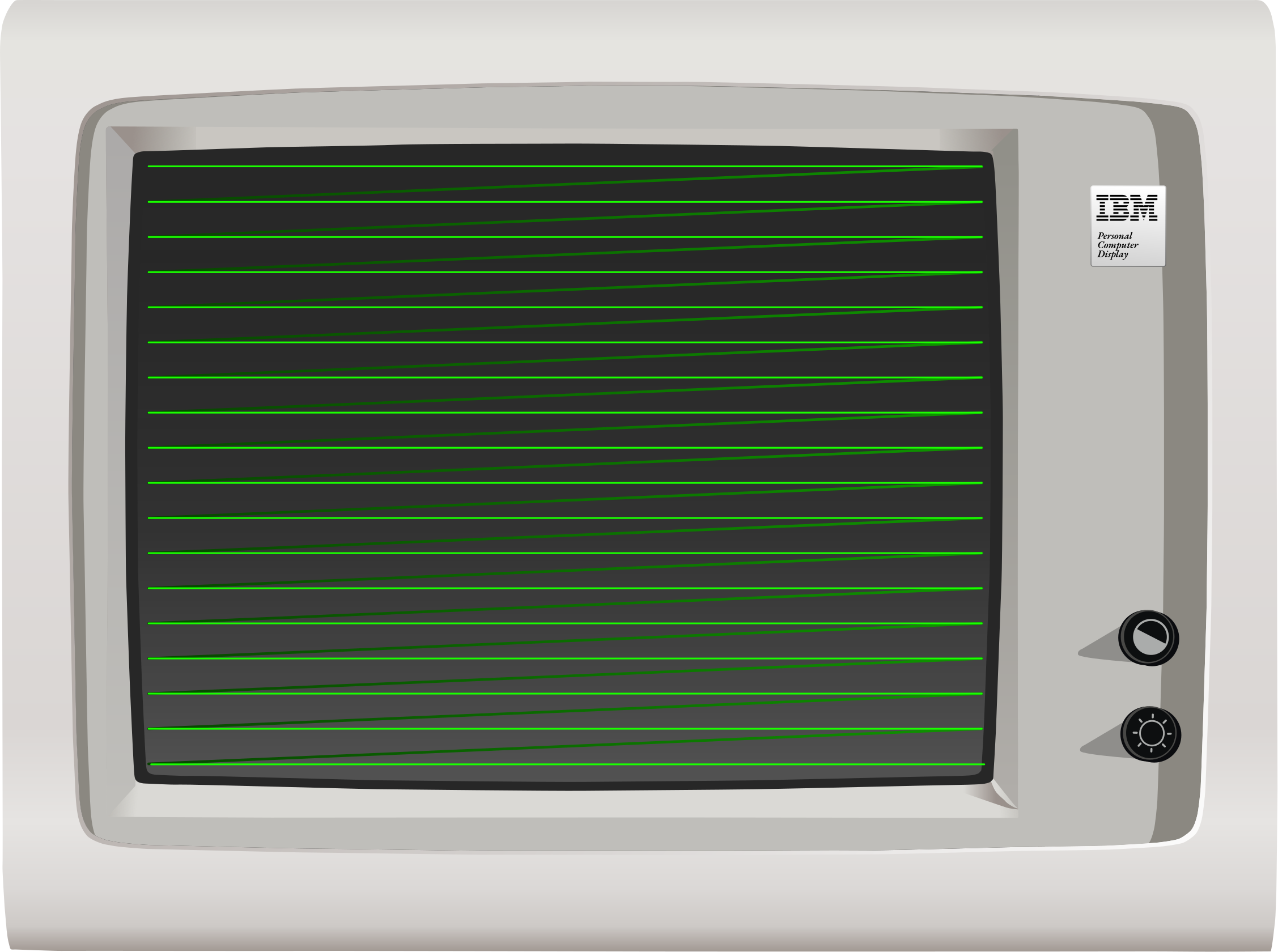
CRT horizontal scanout (Click to zoom)
If unaccounted for, the continuous vertical deflection would cause the image to be rotated slightly, with each scanline ending slightly lower down on the screen from where it started. To counteract this, the entire deflection yoke is mounted with a slight counter-rotation to ensure scanlines remain level.
When the beam has reached the bottom of the screen, vertical retrace occurs, as the electron beam returns to the top of the screen again, and the process repeats. This frequency at which this process occurs is called the vertical refresh frequency, and may be anywhere from 50Hz to 70Hz or more, depending on the adapter and monitor. Horizontal deflection continues throughout vertical flyback - if the beam were left on, it would be seen to ping-pong off the sides of the screen as it returned to the top. Simplified diagrams will often only show the beam moving in a direct diagonal path from one corner to the other.
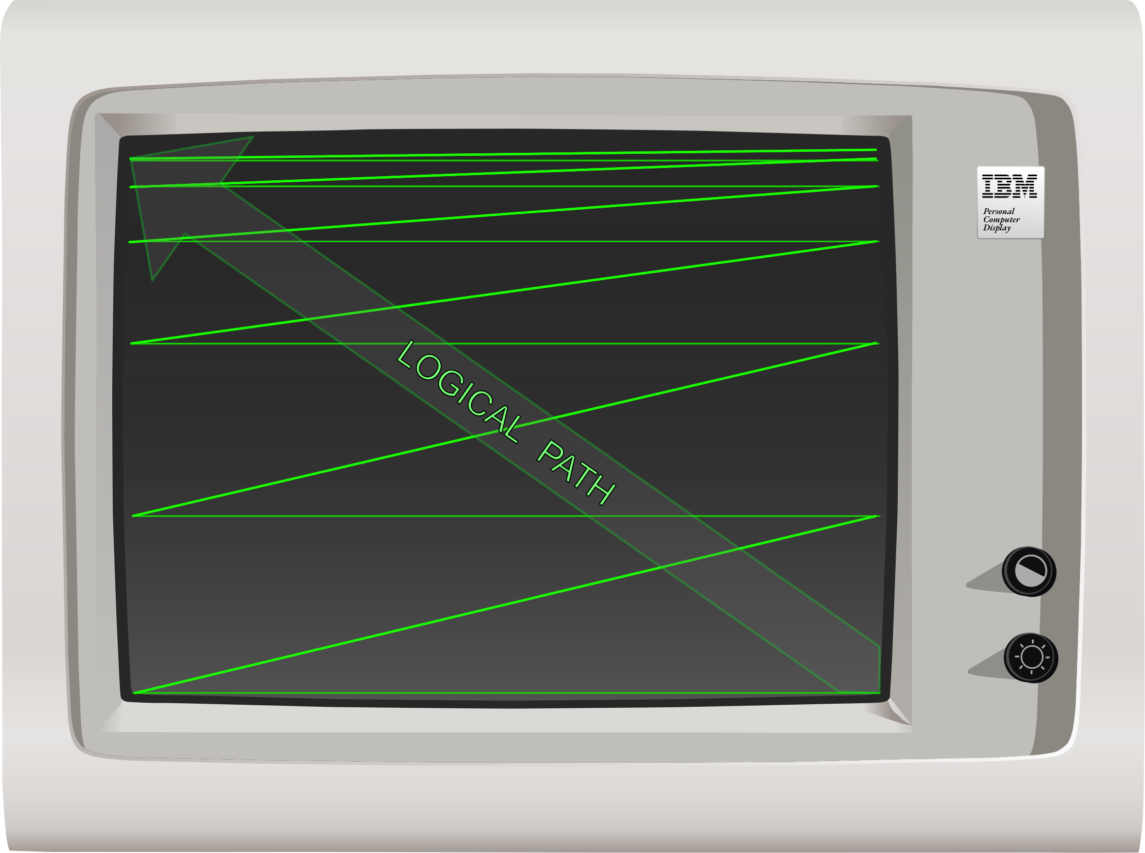
CRT vertical flyback (Click to zoom)
Phosphor Decay
The phosphors on the screen are only fully lit during the period in which the electron beam is directly illuminating them, after which they immediately begin to fade. Different phosphors fade more slowly than others — the phosphors used in older monochrome monitors were long persistence phosphors, meaning they faded slowly enough that scrolling text could leave a smeary after-image or trail on the screen. The long persistence phosphors on monochrome displays made up for slower refresh rates. On color displays, fast-responding phosphors were preferred.
To a high speed camera, a CRT will look like a bright line trailed by a fading image, however a quirk of human perception called persistence of vision means that we perceive the display as having a fixed, steady image. That said, many people experience eye strain using monitors with lower refresh rates.
Color
The previous descriptions and diagrams have shown a monochrome CRT. A color CRT operates in a similar way, but with three electron beams and three sets of phosphors, one for each of the additive primary colors red, green, and blue. The individual beams are guided to their corresponding phosphors through one of several possible mechanisms, most commonly either an shadow mask or aperture grille.
Video Synchronization
A video card emits two synchronization signals, which are represented as pulses of either positive or negative polarity, depending on the current display adapter and mode. These pulses signal to the monitor the video card’s intent that a horizontal or vertical flyback be performed. These are called HSYNC and VSYNC, respectively. Most monitors, in order to protect themselves from honoring invalid or harmful synchronization frequencies, maintain one or more Phase Locked Loops (PLLs), usually implemented via some sort of sync controller IC. This allows the monitor to adapt — or sync — to a range of horizontal and vertical refresh frequencies that it can safely support, while ignoring sync signals that fall outside that range. The monitor’s PLL will cause horizontal or vertical flyback to occur when necessary, regardless of synchronization. That said, some models of monitor lack at least one PLL — such as the IBM 5151 — and can be damaged in the event that the video card sends invalid horizontal synchronization signals.
In general, the monitor’s electron beam cannot be frozen or held in place by the host computer failing to send synchronization pulses. It is constantly moving - if it is not, something has gone very wrong. For most monitors, if the card does not send synchronization signals, the monitor will trigger flyback on its own.
When a monitor fails to achieve vertical synchronization, the picture is typically seen to scroll vertically (and often rapidly) across the screen, a phenomenon called rolling. This is caused by the monitor’s PLL-driven vertical flyback being out of phase with the video signal’s VSYNC pulses. Physical knobs, like the vhold knob, are sometimes provided to assist in adjustment in this case.
When a monitor loses horizontal synchronization, the effect on the picture is much more dramatic, with the image completely scrambled instead of scrolling.
Digital vs. Analog
Video signals can often be described as digital or analog. The digital video signals of the 1980’s were not like those of today. When we talk about a digital video signal in the context of the original PC, it simply refers to TTL-level output on dedicated color and intensity pins. Video cards could sometimes emit both digital and analog signals. The DE-9 connector on MDA, CGA, and EGA cards carries a digital video signal - on the CGA, this signal is converted to an analog composite signal on the card’s composite output jack.
The VGA card introduced analog video to the PC. The VGA’s analog signal allowed a wider range of colors to be displayed without a drastic increase in pin count, by modulating voltage on each pin dedicated to the primary colors instead of relying on discrete intensity pins like with CGA and EGA.
Light Pens
The operation of raster displays allows for a unique and conceptually simple input device to be constructed. A light pen is constructed of a lens, photodiode, and filtering circuitry. When a light pen is held to the surface of a CRT, the photodiode within the tip detects the passing of the electron beam directly beneath it, causing a pulse or strobe signal to be generated. The position of the pen can be calculated on the horizontal axis by the time elapsed since the last HSYNC, and on the vertical axis by counting each scanline. A light pen often had a switch at the tip of the pen that would be pressed when held against the screen to initiate a drawing operation, separate from cursor movement.
Emulation Considerations
It’s not necessary to emulate the way a monitor scans out the screen to emulate the PC, although monitor emulation (emulating the PLLs and synchronization performed by a real monitor) can produce satisfying effects like screen bounce on mode changes. Knowledge of how horizontal and vertical sync pulses work, as well as horizontal and vertical refresh timings, are important for emulating cards such as the EGA and VGA which contain self-tests in their corresponding BIOS ROMs that test for proper operation of these signals.
Terminology
- pixel: - (Picture Element) This is usually the smallest addressable element of a raster display, determined by the capabilities of the display and display adapter.
- hdot: - (Horizontal dot) This is essentially the time-based unit equivalent to a pixel, but a pixel need not be drawn during every hdot.
- dot clock: - The frequency at which the video card produces pixels. By slowing down the dot clock, the effective horizontal resolution of a card can be decreased, making each pixel wider. The display timings of the card must be reconfigured to account for this.
- horizontal blanking period: - The period in which the electron beam is turned off at the left and right edges of the screen or beyond.
- vertical blanking period: - The period in which the display is turned off at the top and bottom edges of the screen or beyond.
- horizontal retrace: - The period in which the electron beam is being moved from the right side of the screen to the left side. Occurs during the horizontal blanking period. Also called a horizontal flyback.
- vertical retrace: - The period in which the electron beam is being moved from the bottom-right of the screen to the top-left side. Occurs during the vertical blanking period. Also called a vertical flyback.
- horizontal front porch: - The period of the horizontal blanking period immediately before the horizontal retrace period.
- horizontal back porch: - The period of the horizontal blanking period immediately after the horizontal retrace period.
- vertical front porch: - The period of the vertical blanking period immediately before the vertical retrace period.
- vertical back porch: - The period of the vertical blanking period immediately after the vertical retrace period.
- HSYNC: - A signal the display adapter sends to the monitor to initiate the horizontal retrace period.
- VSYNC: - A signal the display adapter sends to the monitor to initiate the vertical retrace period.
- horizontal refresh rate: - The frequency at which the monitor displays an entire scanline, ending in an hsync. Expressed in kHz.
- vertical refresh rate: - The frequency at which the monitor displays an entire frame, ending in a vsync. Expressed in Hz.
- overscan:
- On analog television sets, the overscan is part of the video signal that may be hidden by the display’s bezels.
- On digital computer monitors, ‘overscan’ typically refers to the part of the video signal which lies outside of the region where addressable pixels are displayed, which may lie partially within the borders of the monitor’s bezels, and partially outside it. The overscan can often be set to a particular color, depending on the adapter.
Primary References:
- (cosmodoc.org) People Don’t Like Electrons Shooting At Their Face
The Motorola MC6845
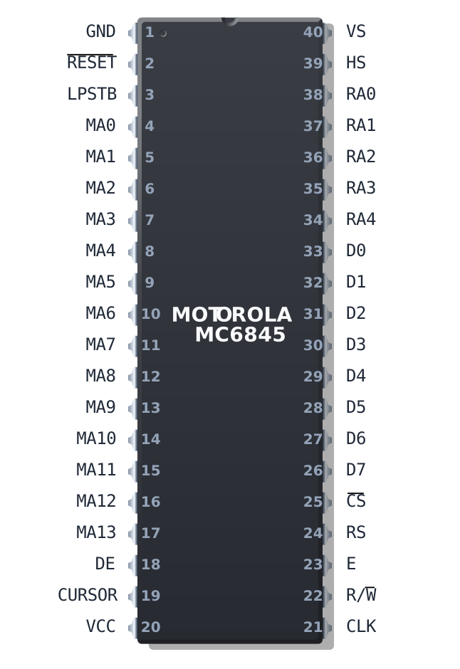
The Motorola MC6845
The Motorola MC6845 is a Cathode Ray Tube Controller (CRTC). Its primary purpose is to generate video memory addresses and video synchronization signals as part of a larger raster display system. It contains a number of registers that together define a specific video frame geometry, and a number of counters that are incremented or decremented while being compared against the values stored in the register file. These comparisons happen continuously, via circuits attached to the registers themselves called coincidence circuits. That’s just a fancy name for a simple equality comparator.
You can see the coincidence circuits in the image below as the green boxes that sit above most of the pink registers.
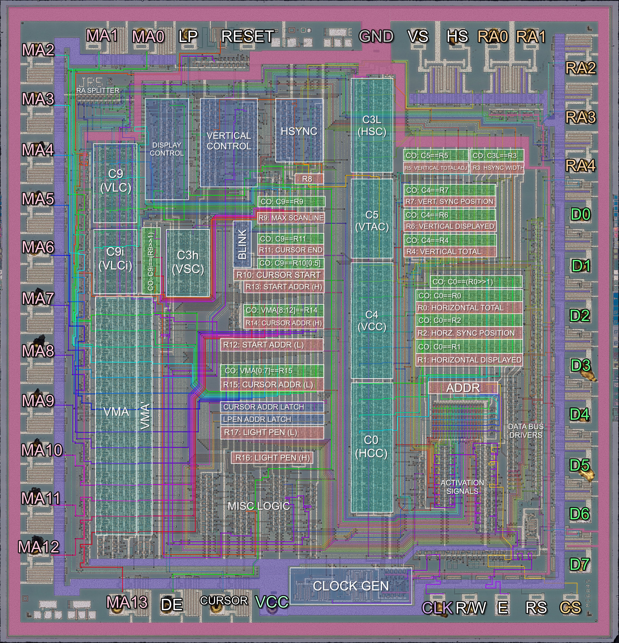
Motorola MC6845 Annotated Die Photo (Click to zoom)
When certain counters coincide (become equal with) certain registers, various logic circuits may be triggered. For example, when the counter that holds the current character-column position becomes equal with the register that holds the total number of characters to be displayed, the MC6845 will indicate via an external pin that the display area has ended for the particular line. In this manner the MC6845 can produce the display timing signals corresponding to the configured frame geometry.
As part of a video card or other display system, these signals trigger further logic on the card itself - for example, the DE or Display Enable pin, might be tied to logic that controls whether the video card outputs graphics data or emits a solid black color. The MC6845’s MA pins will typically be used to address the video card’s video memory.
Character Cell Logic
The MC6845 is fundamentally designed to handle character-based or text mode displays. It assumes that your characters will all be of the same width and height, but they do not need to have exactly equal width and height. The MC6845 can handle characters up to 32 lines tall. In most implementations, a line from the MC6845’s perspective is equal to a scanline on the monitor.
The rectangular bitmaps that define how characters appear on screen are called character glyphs. The MC6845 does not define any margins or spacing between glyphs - the requisite spacing must be encoded into the glyph bitmaps themselves. On the IBM PC, there is typically one pixel of spacing between each character, horizontally and vertically, but in certain circumstances a video card may override this.
Here is a hypothetical example of a row of 6x8 character glyphs:
The MC6845 has no concept of how wide your character glyphs actually are. Most video standards for the PC will define a character that is either 8 or 9 pixels wide, usually producing a horizontal display resolution of 640 or 720 pixels when configured for an 80-column display. But you could have 64 pixel wide characters, or 4096 - the only limits are practicality and memory bandwidth.
If we think about it, the MC6845 leaves us a lot of leeway to provide our own definition of what a ‘character’ even is. We could just as easily use the MC6845 to drive an array of LEDs. It is exactly this sort of flexible representation that allowed graphics vendors using the MC6845 to implement graphics modes on what was a fundamentally character-based chip. To learn more about how that was done, you’ll need to read a chapter that discusses a specific card like the IBM CGA.
The MC6845 has to draw every row of characters several times - as many times as the character height is defined in lines. Each pass through a row draws the subsequent row of pixels of each character glyph. This is controlled by an internal counter C9 (Vertical Line Counter), the contents of which are emitted on the CRTC’s RA pins which in turn can be used to address an external character (font) ROM.
Clocking the MC6845
The MC6845 receives a clock called the character clock which indicates how fast characters should go by on the screen, since that is what the MC6845 is managing. This is typically produced by taking the dot clock input of the card and dividing it by the current character width.
For every new clock edge of the character clock, the MC6845 produces a memory address on its 14 MA address pins.
Memory Address Generation
The MC6845’s address pins provide the address of the character that should be displayed at roughly that instant (ignoring rasterization latency). On each character clock, the internal memory address, a counter called VMA, is either incremented by one, reset, or set to a latched value, depending.
The address emitted by the MC6845 may not be a literal byte address. As discussed above, a character address can be interpreted liberally. In IBM CGA text mode, each character cell is a 16-bit value: pairs of ASCII character codes and CGA attribute bytes. The address may be further manipulated in other ways, sometimes using the RA counter - a common trick to create graphics modes.
MC6845 Registers
The MC6845’s register numbers are frequently given in either decimal or hexadecimal. Motorola’s own references use decimal, so that is what we will use here.
| Index | Hex | Name | Long Name | R/W | Size (Bits) |
|---|---|---|---|---|---|
| - | — | ADDR | Address Register | WO | 5 |
| 0 | 00h | R0 | Horizontal Total | WO | 8 |
| 1 | 01h | R1 | Horizontal Displayed | WO | 8 |
| 2 | 02h | R2 | Horizontal Sync Position | WO | 8 |
| 3 | 03h | R3 | Sync Width | WO | 4 |
| 4 | 04h | R4 | Vertical Total | WO | 7 |
| 5 | 05h | R5 | Vertical Total Adjust | WO | 5 |
| 6 | 06h | R6 | Vertical Displayed | WO | 7 |
| 7 | 07h | R7 | Vertical Sync Position | WO | 7 |
| 8 | 08h | R8 | Interlace Mode and Skew | WO | 2 |
| 9 | 09h | R9 | Max Scan Line Address | WO | 5 |
| 10 | 0Ah | R10 | Cursor Start | WO | 7 |
| 11 | 0Bh | R11 | Cursor End | WO | 5 |
| 12 | 0Ch | R12 | Start Address (High) | WO | 6 |
| 13 | 0Dh | R13 | Start Address (Low) | WO | 8 |
| 14 | 0Eh | R14 | Cursor Address (High) | RW | 6 |
| 15 | 0Fh | R15 | Cursor Address (Low) | RW | 8 |
| 16 | 10h | R16 | Light Pen Latch Address (High) | RO | 6 |
| 17 | 11h | R17 | Light Pen Latch Address (Low) | RO | 8 |
The MC6845 has two IO ports - an address port, and a data port. One should first select a register via the address port, which is done by holding the RS pin low. This is an electrical detail you are unlikely to need to emulate - the card on which the MC6845 has been included will decode a separate IO address for the MC6845’s address and data register. See the chapter for the specific card you are emulating. From the CGA onwards, the CRTC registers are at 3D4h and 3D5h.
The address register, being 5 bits wide, will happily hold any value from 0-31, meaning an invalid selection may be stored. In this scenario, writing to the data register has no effect, and reading from the data register is ultimately implementation-specific but likely to return either 0x00 or 0xFF. The chapter for a specific card may have more details.
Most of the registers simply contain integer values, but pay close attention to their bit lengths, and perform the appropriate masking when writing to them.
Two exceptions to this rule are R8, which contains two flags relating to interlaced video, and R10, which contains two additional bits that control cursor blinking. Their formats are given here.
Interlace Mode and Skew
| Bits | Name | Description |
|---|---|---|
| 0 | IS | Interlaced Sync (0=Normal, 1=Interlaced) |
| 1 | IV | IV: Interlaced Video (0=Normal, 1=Interlaced)* |
| 2:7 | Unused | Unused |
IV: Interlaced Video (0=Normal, 1=Interlaced)*
*Note: The IV bit is only meaningful if the IS bit is set. Otherwise it is ignored.
| IV | IS | Mode |
|---|---|---|
| 0 | 0 | Normal sync and video |
| 1 | 0 | Normal sync and video |
| 0 | 1 | Interlaced sync only |
| 1 | 1 | Interlaced sync and video |
Cursor Start Register
| Bits | Name | Description |
|---|---|---|
| 0:4 | CUR_START | Cursor Start Line |
| 5 | P | Blink Period |
| 6 | B | B: Blinking Enable |
| 7 | Unused | Unused |
B: Blinking Enable
| B | P | Cursor Display Mode |
|---|---|---|
| 0 | 0 | Non-blink |
| 0 | 1 | Cursor non-display |
| 1 | 0 | Blink at 1/16 field rate |
| 1 | 1 | Blink at 1/32 field rate |
Don’t worry about the meaning of the fields in these registers just yet. The register definitions are provided here for completeness with the register table reference.
MC6845 Counters
| Name | Description | Bits | Compared to |
|---|---|---|---|
| C0 | HCC (Horizontal Character Counter) | 8 | R0,R1,R2 |
| C9 | VLC (Vertical Line Counter) | 5 | R9,R10,R11 |
| C9.IVM | VLCi (Vertical Line Counter, Interlaced) | 4 | R9>>1 |
| C4 | VCC (Vertical Character Counter) | 7 | R4,R6,R7 |
| C3h | VSC (Vertical Sync Counter) | 4 | Fixed: 16 |
| C3l | HSC (Horizontal Sync Counter) | 4 | R3 |
| C5 | VTAC (Vertical Total Adjust Counter) | 5 | R5 |
| VMA | Video Memory Address Counter | 14 | R12,R13,R14,R15 |
The table above shows the various counter units on the MC6845. They will be largely referred to here by their names in the Name column. If you read the source for other emulators, you may encounter names given in the Description column. The new names for these counters come from the Amstrad CPC CRTC Compendium.
Latches and Flags
The MC6845 has an important latch which is referred to as VMA' or VMA Prime. VMA' can be loaded with the value of the VMA counter, and the VMA counter can be loaded with either VMA' or the contents of the Start Address registers, R12 and R13.
You can see the VMA' latch as the tall vertical section immediately to the right of the VMA counter in the die photo above.
Besides the VMA' latch, there are various bits of state that the MC6845 can keep as flags. These include a last_line flag.
Defining a Frame
A frame is a single image displayed on a CRT monitor, typically delineated by VSYNC pulses. See Display Concepts if this isn’t already a familiar concept. The role of the MC6845 is managing the size and timings that define a single frame. The MC6845’s registers define these parameters, and its counters are used to actually play out said timings - a process I will refer to as scanout.
The most important concept to grasp when understanding how the MC6845 defines a frame is that it is not just defining the position and size of visible elements, but also timings for invisible events such as horizontal and vertical sync periods. It can be helpful to think of a MC6845 frame as a two dimensional time chart, or field diagram - this allows us to map areas where the raster beam may be moving around as simply a region of time. This book will often discuss this imaginary display field, and you may need to frequently refer back to this diagram for reference.
The diagram below demonstrates the typical parameters used to implement the standard 80x25 text mode display on an IBM CGA card.
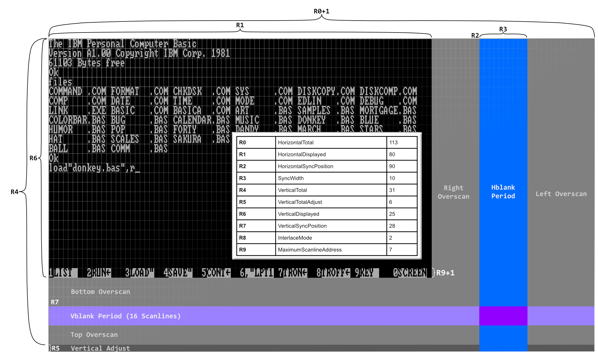
The CRTC Display Field Diagram (Click to zoom)
Frame Extents
The two-dimensional extents of the display field are defined by R0 and R4. They represent the width and height of the field, respectively, minus one.
The extents of the display area are given by R1 and R6. These contain the exact width and height of the display area. In the diagram above, you can see they are programmed for 80 and 25, as expected.
The other parameters set up the positions (and sizes, where applicable) of the horizontal and vertical blanking/sync periods, which overlap each other, as several horizontal syncs will occur during vertical blanking.
The rest of the screen is a sort of no-man’s land we call the overscan. Some video cards will let you emit a solid color here. Not all cards have such large overscan areas.
It may not be possible to produce a screen using just a multiple of your character height that satisfies display requirements, such as NTSC’s specification of 262 scanlines. For example, a field of 32 rows (R4 == 31), with 8 scanline tall characters, only produces 256 scanlines. This may cause trouble with your monitor’s vertical synchronization circuitry. Thus the register R5 is provided to pad out the end of the frame by the indicated number of scanlines - in the above case, 6, until a full 262 scanlines are emitted.
MC6845 Outputs
While still referring to the diagram, note that the MC6845 will raise its HS pin when it is within the blue hblank period. It will raise its VS pin when it is in the lighter blue vblank period. Both pins will be asserted when these periods intersect.
While the MC6845 is scanning out the region defined by R1 and R6, it will assert its DE (Display Enable) pin, which should drive rasterization of text or graphics by the attached display system.
Scanning out a Frame
The process of scanning out the frame or display field may be considered to start in the upper left corner of the display area.
C0 and C4, our horizontal and vertical character counters will both be 0.
C9, our vertical line counter - indicating what row of a character we are drawing - will also be 0.
At the beginning of a frame, the MC6845 performs Start-Of-Frame Management.
Start-Of-Frame Management
The VMA counter is loaded with the 14-bit start address taken from the R12 and R13 start address registers.
The VMA' latch is loaded with the same address at this time. Note that as VMA counts, VMA' retains the same value unless updated by some other event.
We will start in the active display area, so DE will be high.
Scanning out a Row
Every character clock, a number of comparisons are made that trigger various state changes. It may be helpful to think of these as occurring before the increment of any counter.
- If
C0 == R1, we leave the active display area and enter the right overscan period. - If
C0 == R2, we enter the horizontal sync period, which we will gloss over for the moment. - If
C0 == R0, we have reached the far end of the display field.- If
C9 == R9, we are on the last scanline of a row, in which case we enter End-Of-Row Management. - Otherwise,
C9is incremented,VMAis updated withVMA'(to reset the memory address to the start of the row again), and the process repeats.
- If
Each row is scanned out R9 + 1 times. In our 80x25 text mode example, we can see that R9 is 7. Therefore each row will consist of 8 scanlines.
Frame Scanout, Visualized
The logic above for scanning out rows is repeated. During End-Of-Row Management, C4 is incremented. When C4 == R4 we have reached the end of the screen. At this point, if R5 is nonzero, C5 will be initialized with R5 and the MC6845 will start scanning out R5 scanlines in the Vertical Total Adjust Period. When this has elapsed, or if R5 was zero, the frame ends and a new frame immediately begins.
You can see an animation of the full frame scanout process below, with certain internal counters visualized.
Cursor Management
The MC6845 has a hardware cursor, with a dedicated CURSOR pin. This pin is typically active during character clocks when the current VMA matches the value configured by the Cursor Address Registers (R14 & R15) and the current value of C9 is within the range defined by the Cursor Start (R10) and Cursor End (R11) registers.
The CURSOR signal will be suppressed for several frames for the same memory location as the cursor blinks off, unless blinking has been disabled.
In a normal scenario, Cursor Start is programmed for a value less than Cursor End, and the cursor is drawn from the scanline represented by Cursor Start up to and including the scanline represented by Cursor End. If Cursor Start and Cursor End are equal, the cursor will be drawn for a single scanline.
The cursor on the IBM PC is usually two scanlines tall.
The cursor is typically configured to appear at the bottom of a character cell, but nothing prevents you from placing it at the top:
Hiding the Cursor
There are three primary ways of hiding the cursor on a MC6845-based video card:
- You can set the cursor address to a memory address outside of the current display area.
- You can set the Cursor Start register to a value greater than
R9. - You can set the blink bits to
01in the Cursor Start register.
Cursor Tricks
Some odd things happen when you start playing around with non-standard configurations of cursor start and end.
If you set the value of Cursor End > R9, then a full-block cursor is created.
More unexpectedly, if you configure Cursor End < Cursor Start < R9, you can get a “split” cursor:
The explanation for this behavior is really quite simple. The MC6845 has an internal flag that we will call Cursor Active (CA). The cursor is not evaluated per character cell, it is evaluated per scanline. When we reach the end of each scanline while scanning out a row, the MC6845 checks if the new row scanline matches the value in Cursor Start. If it does, the CA flag is turned on. In a similar fashion, if the outgoing row scanline matches Cursor End, the CA flag is turned off.
What is important to understand here is that these comparisons against the cursor start and end are all that controls this global cursor flag. It is not reset upon VSYNC, or new frames.
Let’s reexamine the case of the solid block cursor. By configuring Cursor End > R9, we ensure that the comparison that would otherwise turn the cursor off, can never be true. Therefore the CA flag is turned on, and stays on permanently. However, the cursor is only actually visible in the bounds of a single character cell when VMA matches the Cursor Address.
By making Cursor End < Cursor Start it should now be clear that this reverses or “inverts” the cursor definition. Instead of turning on and then off within a character row, it turns off and then on - remaining on as we proceed to the next row. In this sense, the cursor is now spanning across two rows at a time - it isn’t “split” at all, it just appears that way given the limited aperture of a single character cell.
Ultimately, cursor visibility is a combination of CA AND VMA == Cursor Address AND NOT blink.
Important
The
CAflag is not updated during the vertical total adjust period.
Interlaced Mode
For most of the PC’s history, the MC6845’s interlaced mode was not used. On the IBM CGA, IBM even took measures to make sure it was nonfunctional. Only recently have demoscene coders started exploring the use of interlaced mode for various effects. This section will be expanded in the future.
Light Pen
The MC6845 has basic support for light pens. The chip’s physical LPSTB or light pen strobe pin is a positive-edge-triggered input, that causes the current VMA to be written to R16 and R17. This is an asynchronous input signal that can occur any time, so presents a bit of challenge for an otherwise synchronous chip. The exact electrical details are not particularly important. Heed Motorola’s warning that the address ultimately latched may be some character clocks distant from when the strobe actually fired. In experience, on an IBM CGA card, this produces a cursor offset of 5-6 character clocks before calibration.
Most light pen-supporting programs and light pen drivers will have calibration routines to offset this delay.
The LPSTB input is not latched - every time there is a rising edge a new address will overwrite the values of R16 and R17. If this is not desired, a card maker may place a resettable flip-flop in between the light pen’s strobe input and the MC6845 LPSTB pin. Since most light pen strobe inputs are active-low, an inverter is typically employed as well.
Datasheet
- (archive.org) Motorola MC6845
Primary References
- (shaker.logonsystem.eu) The Amstrad CPC CRTC Compendium V1.9
Additional Watching
- (youtube.com) Visiting Area 5150
Monochrome Display Adapter (MDA)
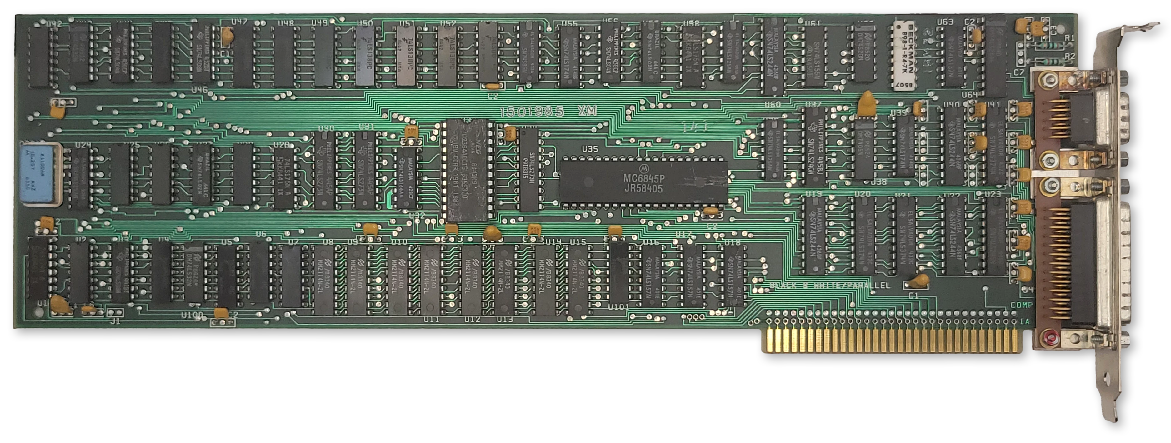
The IBM MDA card
The IBM Monochrome Display Adapter (MDA) was one of the first video adapters available for the IBM PC, along with the IBM Color Graphics Adapter and the third-party Hercules video adapter.
Important
The MDA is built around the Motorola MC6845 CRTC. Read that chapter first for a basic understanding of how the CRTC is used to define frame geometry and draw the screen.
At a Glance
| Item | Description |
|---|---|
| Video memory | 4KiB at B000:0, mirrored 8x through B700:0 |
| Expansion ROM | None |
| Font ROM | 8KiB Character generator ROM, 8x14 glyphs |
| Main display outputs | TTL monochrome video on DE-9, |
| Typical text modes | 80x25, 4 shades, 9x14 character cell |
| Standard Resolution | 720x350 @ 50Hz |
| Standard graphics modes | None |
| I/O address range | 3B0h-3BFh |
| CRTC address port | 3B4h standard, 3B0h, 3B2h, 3B6h alternate* |
| CRTC data port | 3B5h standard, 3B1h, 3B3h, 3B7h alternate* |
| MDA control ports | 3B8h mode control |
| MDA status port | 3BAh |
| Parallel port | 3BCh-3BEh |
| Interrupts | No display interrupt; printer interface uses IRQ7 |
| DMA | None |
The MDA was intended for use with the IBM 5151 Personal Computer Display. This monitor plugged into the back of the PC’s power supply and turned on and off with the system. The MDA card itself was only capable of displaying text mode, but the monitor itself could display graphics, which cards like the Hercules Graphics Adapter took advantage of to provide a tempting upgrade for 5151 owners.
The MDA has 4KiB of DRAM dedicated to video memory — enough to hold a single 80x25 screen’s worth of text. It also has an 8KiB font ROM that holds bit patterns for drawing text glyphs.
The MDA’s 4KiB of DRAM at segment B000:0 is incompletely decoded, causing eight mirrors of video memory from B000:0 through B700:FFFF. This ends at the CGA’s memory address of B8000. Along with the different base IO address, this allowed one to install both an MDA card and a CGA card in the same system for an early dual-monitor setup.
The MDA has no on-board video BIOS or expansion ROM. All PC-compatible BIOS implementations must therefore know how to identify, initialize and operate an MDA card in order to provide standard int 10h services.
In text mode, the MDA card was capable of outputting 3 grayscale shades and black, using two output pins of its DE-9 video connector. Some early MDA cards could be coerced into showing 16 colors.1
The MDA contains a 16.257MHz crystal. The refresh rate is approximately 50Hz.
The IBM MDA card included a parallel printer port. See that section for more details.
Note
* Incomplete decoding of the CRTC registers means the two CRTC ports are repeated four times. Some software titles may rely on these alternate port numbers.
MDA Character Glyphs (Standard Font)
The standard MDA character glyphs are shown below.
| 0 | 1 | 2 | 3 | 4 | 5 | 6 | 7 | 8 | 9 | A | B | C | D | E | F | |
|---|---|---|---|---|---|---|---|---|---|---|---|---|---|---|---|---|
| 0 | ||||||||||||||||
| 1 | ||||||||||||||||
| 2 | ||||||||||||||||
| 3 | ||||||||||||||||
| 4 | ||||||||||||||||
| 5 | ||||||||||||||||
| 6 | ||||||||||||||||
| 7 | ||||||||||||||||
| 8 | ||||||||||||||||
| 9 | ||||||||||||||||
| A | ||||||||||||||||
| B | ||||||||||||||||
| C | ||||||||||||||||
| D | ||||||||||||||||
| E | ||||||||||||||||
| F |
A visualization of the character font ROM is shown below, with bytes reversed and wrapping vertically to fit into a square image. The first half of the ROM is dedicated to the MDA’s 8x14 font, which is encoded into 8x16 cells for alignment. Each cell is split into two 8x8 parts within the ROM due to addressing logic.
The same character ROM image is used for both MDA and CGA, so the CGA fonts follow the MDA font in the latter half of the ROM.
The MDA/CGA character font ROM (byte-reversed)
The character font ROM is not accessible from the host PC. It can only be read by the MDA itself.
Box Drawing Characters
Character codes C0h—DFh receive special treatment. When one of these characters is being rasterized, the eighth column is repeated to form the ninth column on the display. This allows the box drawing characters to connect seamlessly together across a 9-pixel character cell.
MDA box drawing character rendering
Note that B0h—B2h do not receive this treatment, so areas shaded with these characters will still have one pixel gaps between each character glyph.
The MDA Registers
Mode Control Register
| Bits | Name | Description |
|---|---|---|
| 0 | HIRES | High-Resolution Mode 0: Not implemented; must not be set. 1: High-resolution mode (normal operation) |
| 1 | B/W | Black-and-White Mode Value written is not used. |
| 2 | Unused | Unused |
| 3 | VIDEO | Video Enable 0: Video output disabled 1: Video output enabled |
| 4 | Unused | Unused |
| 5 | BLINK_EN | Text Blinking Control 0: Attribute bit 7 controls background intensity1: Attribute bit 7 controls blinking |
| 6:7 | Unused | Unused |
Caution
IBM warns that the first thing that must be done to initialize the MDA is to set bit 0 of the mode control register to 1.
Bit 0 of the mode control register selects the MDA’s dot clock. When set to 1, the onboard 16.257MHz crystal is used. If set to 0, the clock is taken from an unpopulated pad. If the MDA’s video memory is accessed while this bit is 0, the MDA card will fail to drive the IO_CH_READY pin on the ISA bus high, and the CPU will hang. It is unclear what IBM’s original intent for implementing this was, but perhaps they were simply keeping their options open for a future variant that supported additional resolutions and would have subsequently required a second clock source.
Status Register
| Bits | Name | Description |
|---|---|---|
| 0 | RETRACE | Horizontal retrace status 0: Horizontal retrace is inactive 1: Horizontal retrace is active |
| 1 | LPT | Light-pen trigger state (early revision only) 0: Light pen trigger has not fired 1: Light pen trigger has fired. |
| 2 | LPS | Light-pen switch status (early revision only) 0: Light pen switch on 1: Light pen switch off. |
| 3 | LVIDEO | Video output status latch 0: No active pixel is being output (black) 1: An active pixel is being output (normal or bright pixel) |
| 4:7 | Unused | Unused: Always Fh. |
The MDA’s status register is very different from the CGA. The first bit reflects the HS pin from the 6845, delayed by one character clock. This differs from the CGA, which reports the inverted DE pin from the 6845.
The MDA also lacks the vertical sync status bit. Instead, it has a type of video mux bit, LVIDEO. Querying bit 3 can test if an active pixel of any “color” other than black is being output. The IBM BIOS primarily uses this as a test during POST to ensure that the card is functioning.
Tip
When writing MDA emulation, implementing the LVIDEO bit may seem daunting. It is generally sufficient to set the latch if any pixel was output in the previous character clock (or even scanline) instead of requiring pixel-perfect accuracy. The IBM BIOS draws a row of solid block characters and tests that the bit is set immediately at the start of the frame. It is unknown if any software besides the BIOS POST relies on this bit for proper functionality.
Light Pen
The very earliest models of the MDA card include a header to attach a light pen, similar to the CGA. This was removed on all subsequent versions of the card — the entire footprint was removed, not just left unpopulated, and in addition, the strobe signal to the 6845 and the two status bits for light pen operation were also disconnected and will always return 0.
The P39 phosphors used in most monochrome displays were incompatible with early light pens for the PC, which may have influenced IBM’s decision to remove light pen support from the MDA.
Display Timings
The MDA has a 16.257MHz crystal.
We can calculate the typical display field of the MDA from its normal CRTC parameters:
$$H_{\text{total}} = (R0 + 1) \times 9 = (97 + 1) \times 9 = 882$$
$$V_{\text{total}} = (R4 + 1) \times (R9 + 1) + R5 = (25 + 1) \times 14 + 6 = 370$$
$$\text{display field} = 882 \times 370$$
The horizontal and vertical refresh rates can then be derived:
$$f_{hsync} = \frac{16{,}257{,}000}{882} = 18.43 \text{ kHz}$$
$$f_{refresh} = \frac{16{,}257{,}000}{882 \times 370} = 49.82 \text{ Hz}$$
BIOS Video Mode
The MDA typically uses standard int10h video mode 7.
CRTC Parameters
For the MDA’s standard text mode, the MC6845 CRTC needs to be configured with the correct parameters for registers R0-R11. The standard CRTC parameters are given below.
| Register | Name | Text Mode |
|---|---|---|
| 80 Column | ||
| R0 | HorizontalTotal | 97 |
| R1 | HorizontalDisplayed | 80 |
| R2 | HorizontalSyncPosition | 82 |
| R3 | SyncWidth | 15 |
| R4 | VerticalTotal | 25 |
| R5 | VerticalTotalAdjust | 6 |
| R6 | VerticalDisplayed | 25 |
| R7 | VerticalSync | 25 |
| R8 | InterlaceMode | 2 |
| R9 | MaximumScanLineAddress | 13 |
| R10 | CursorStart | 11 |
| R11 | CursorEnd | 12 |
Primary References
- (seasip.org) Monochrome Display Adapter: Notes
- (minuszerodegress.net) IBM Monochrome Display and Printer Adapter (MDA)
-
VCFed forum thread, Why did IBM create color MDA and just abandoned it?, April 2025. ↩
The IBM Color Graphics Adapter
The IBM CGA card
The IBM Color Graphics Adapter (CGA) was one of the first video adapters available for the IBM PC, along with the IBM Monochrome Display Adapter and the third-party Hercules video adapter. It is perhaps the classic video card that comes to mind when people think of the IBM PC.
Important
Like the MDA, the CGA is built around the Motorola MC6845 CRTC. Read that chapter first for a basic understanding of how the CRTC is used to define frame geometry and draw the screen.
At a Glance
| Item | Description |
|---|---|
| Video memory | 16KiB at B800:0000; mirrored at BC00:0000 |
| Expansion ROM | None |
| Font ROM | 8KiB character generator ROM |
| Main display outputs | TTL RGBI on DE-9; NTSC composite video jack |
| Typical text modes | 40x25 and 80x25, 16 colors, 8x8 character cell |
| Standard graphics modes | 320x200, 4 colors; 640x200, 2 colors |
| Standard resolution | 640x200 @ 60Hz |
| Field Resolution | 912x262 |
| I/O address range | 3D0h-3DFh |
| CRTC address port | 3D4h standard, 3D0h, 3D2h, 3D6h alternate* |
| CRTC data port | 3D5h standard, 3D1h, 3D3h, 3D7h alternate* |
| CGA control ports | 3D8h mode control, 3D9h color control |
| CGA status port | 3DAh |
| Light pen latch ports | 3DBh clear latch, 3DCh preset latch |
| Interrupts | None |
| DMA | None |
The CGA could be connected to a regular North American television set via its composite output connector, although most sets of the time would require an RF modulator to do so. A DE-9 connector provided a digital RGBI signal that could be used with an IBM 5153 Color Display. IBM left owners of the CGA waiting a bit for that particular monitor - it was only released in 1983, two years after the CGA’s debut.
The CGA has 16KiB of DRAM dedicated to video memory, and an 8KiB font ROM that holds bit patterns for drawing text glyphs.
The CGA’s 16KiB of DRAM at segment B800:0 is incompletely decoded, causing a mirror of video memory that begins at BC00:0. You can use this mirroring to your advantage in certain circumstances.
The CGA has no on-board video BIOS or expansion ROM. All PC-compatible BIOS implementations must therefore know how to identify, initialize and operate a CGA card in order to provide standard int 10h services.
In text mode, the CGA card was capable of outputting 16 colors. In graphics mode, it was limited to 3 palettes of 3 fixed colors each, with a selectable background color. The CGA also had a high-resolution mode, with a single, selectable foreground color on black.
The CGA’s standard display resolution is 640x200 at a refresh rate of approximately 60Hz.
The CGA maps the MC6845’s two external registers at address 03D4h for the address register and 03D5h for the data register.
Note
* Incomplete decoding of the CRTC registers means the two CRTC ports are repeated four times. At least one known game, Prohibition, relies on this incomplete decoding.
Operational Modes
The CGA has three primary modes of operation: text mode, medium-resolution graphics mode, and high-resolution graphics mode. A brief overview of each mode follows; each will be covered in greater depth later on.
Text Mode
In text mode, the screen is constructed from a grid of character glyphs. IBM called this mode Alphanumeric Mode (A/N) in documentation.
The IBM PC boots into text mode, either in 40-column or 80-column mode depending on how certain DIP switches are set. 40-column mode makes each glyph twice as wide due to a halved dot clock. It was primarily intended for use with television sets, on which 80-column text was difficult to read. Various tweaked text modes were derived by inventive coders over the years that provided a different number of rows and columns, so these extents are not set in stone.
The standard text modes have black and white and color mode variants, although this typically only controls color when using the composite output. The background and foreground color of each character cell can be controlled via attribute bytes.
In text mode, a blinking, hardware cursor is usually shown indicating where the user can type - or if the programmer doesn’t bother hiding it, where the screen was last updated.
CGA 80-column text mode - MS-DOS 5.0 EDIT
Medium Resolution Graphics Mode
In medium-resolution graphics mode, the screen is composed of a 320x200 grid of pixels. IBM called graphics mode All-Points-Addressable (APA) mode.
This is perhaps the most famous mode of the CGA, especially its cyan-magenta-white palette as seen in games like Alley Cat.
In this mode, three basic ‘palettes’ are available, two of which are notorious for being ugly. These are not actually palettes as they are typically understood - more on that below. What might be thought of as index 0, specifies the background color. The background color is usually black, but can actually be chosen from any of the CGA’s 16 possible colors. Careful use of this “extra” palette entry can create interesting effects that also extend into the borders (or overscan) of the screen. Games could use this color to indicate status, such as flashing it red to indicate your player character had taken damage. The color would create a frame around the addressable display area that could have a surprisingly dramatic effect.
The cursor is disabled in this mode.
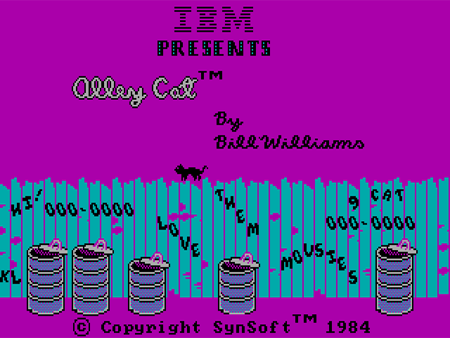
CGA 320x200 graphics mode - Alley Cat by Bill Williams
High Resolution Graphics Mode
This mode provides a very stretched 640x200 monochromatic graphics mode. The foreground color used to draw can be selected from any of the 16 available CGA colors, but the background cannot be changed from black. This mode can be used, with the color burst turned on, to enable 16-color composite artifact color modes.
The cursor is disabled in this mode.
CGA 640x200 graphics mode - SHUTTLE.BAS
The RGBI Color Gamut
The CGA has a digital DE-9 output connector. To produce color, the CGA controls four output pins — one for each of the primary colors: Red, Green, and Blue, along with an “intensity” signal. Four bits give us \(2^4\) or 16 possible colors. The intensity pin provides a repeat of the first eight colors, but brighter.
The odd duck out here is non-intensified yellow, which has been conspicuously darkened to become brown. This was a deliberate decision by IBM, who perhaps found the rather sickly dim yellow unpleasant, or at least believed that a brown color would be more useful. Speculation abounds, but the interesting thing to note is that the conversion circuit to turn yellow into brown is not actually present on the CGA at all - the circuitry is within the IBM 5153 Color Display itself, and third party PC-compatible monitor manufacturers largely followed suit. You may see the original yellow color instead on some non-CGA compatible monitors.
| Decimal | R | G | B | I | Color | Hex |
|---|---|---|---|---|---|---|
| 0 | 0 | 0 | 0 | 0 | 000000 | |
| 1 | 0 | 0 | 1 | 0 | 0000AA | |
| 2 | 0 | 1 | 0 | 0 | 00AA00 | |
| 3 | 0 | 1 | 1 | 0 | 00AAAA | |
| 4 | 1 | 0 | 0 | 0 | AA0000 | |
| 5 | 1 | 0 | 1 | 0 | AA00AA | |
| 6 | 1 | 1 | 0 | 0 | AA5500 | |
| 7 | 1 | 1 | 1 | 0 | AAAAAA | |
| 8 | 0 | 0 | 0 | 1 | 555555 | |
| 9 | 0 | 0 | 1 | 1 | 5555FF | |
| 10 | 0 | 1 | 0 | 1 | 55FF55 | |
| 11 | 0 | 1 | 1 | 1 | 55FFFF | |
| 12 | 1 | 0 | 0 | 1 | FF5555 | |
| 13 | 1 | 0 | 1 | 1 | FF55FF | |
| 14 | 1 | 1 | 0 | 1 | FFFF55 | |
| 15 | 1 | 1 | 1 | 1 | FFFFFF |
In text mode, any of these sixteen colors can be referenced within a character attribute byte.
In graphics modes, the CGA operates in what we might term direct color mode, where the bits set in video memory directly influence the Red and Green output pins.
The CGA only has one true palette register as we typically define one, as in a register that holds an arbitrary color. It is the background/overscan color field in the Color Control Register.
The CGA Registers
Mode Control Register
| Bits | Name | Description |
|---|---|---|
| 0 | HIRES | 80-Column Text Mode Timings Enabled: 0: Normal Timings 1: 80-column Timings |
| 1 | GFX | Display Mode: 0: Text 1: Graphics |
| 2 | B/W | Black-and-White Mode 0: Enable color burst 1: On composite output, disables the color burst. In medium-resolution graphics mode, selects the alternate red/cyan/white palette. |
| 3 | VIDEO | Enable Video Serializers 0: Video Serializers Disabled 1: Video Serializers Enabled |
| 4 | HIRES_GFX | High-Resolution Graphics MUX Control: 0: Disabled 1: High-Resolution Graphics Mode Enabled |
| 5 | BLINK_EN | Text Blinking Control 0: Attribute bit 7 controls background intensity1: Attribute bit 7 controls blinking |
| 6:7 | Unused | Unused |
The CGA Mode Register generates the main control signals that drive the logic of the card. Most descriptions of what these bits do, even in IBM’s own references, only give you an approximation of their actual function. To enter a standard graphics mode, besides reprogramming the CRTC, the correct mode bits must be set.
- The HIRES bit enables the 14.31818MHz dot clock and high-resolution character clock for 80-column text mode. It should not be used in conjunction with the GFX or HIRES_GFX bits.
- The GFX bit enables graphics mode, and triggers replacement of memory address
A13withRA0; a further explanation is given in the medium-resolution graphics section. - The B/W bit disables the composite color burst. It will produce a black and white or grayscale image on a composite monitor or television set. RGBI displays such as the IBM 5153 Color Display will still display color as normal with this bit set, although a third graphics palette can be selected via this bit in medium-resolution graphics mode.
- The VIDEO bit is described by IBM as disabling the video signal - this is not accurate. This bit pulls low the \(\overline{\mathrm{CLR}}\) pins of the CGA’s graphics serializers, U7 and U8. The effect of this is the appearance that all video memory contains
0. This often does result in a black screen, but where conditions allow display of color, such as the border/overscan color being set, color will still be displayed. - The HIRES_GFX bit enables logic on the card to rapidly enable and disable the CGA’s color multiplexers. This bit should not be used in conjunction with HIRES or the text on the screen will become corrupted.
There are several combinations of mode bits that are invalid, and may have strange and interesting effects.
| Mode Bits | Display Mode | Effect |
|---|---|---|
00100 | Mode 0 | 40-Column, B/W Text Mode |
00000 | Mode 1 | 40-Column, Color Text Mode |
00101 | Mode 2 | 80-Column, B/W Text Mode |
00001 | Mode 3 | 80-Column, Color Text Mode |
00011 | invalid | Glitched mode: “Text and Graphics” |
00010 | Mode 4 | 320x200 Graphics Mode |
00110 | Mode 5 | 320x200 Graphics Mode (Alternate Palette) |
10110 | Mode 6 | 640x200 Graphics Mode |
10001 | Invalid | Glitched mode: Text Mode with black bars |
| Bits | Name | Description |
|---|---|---|
| 0 | B | Blue component of the border/background color |
| 1 | G | Green component of the border/background color |
| 2 | R | Red component of the border/background color |
| 3 | I | Intensity component of the border/background color |
| 4 | PAL_I | Drives the Intensity signal in graphics mode, effectively creating a brighter version of the current palette. |
| 5 | PAL_B | Drives the Blue signal in graphics mode, effectively creating a new palette. |
| 6:7 | Unused | Unused |
The color control (or color select) register contains the CGA’s only real color palette entry - an RGBI color may be specified that provides the background/overscan color. This color definition has three distinct use cases - in text mode, it provides the border/overscan color. In medium-resolution graphics mode, it provides the color to use when a pair of bits are both 0, in addition to providing the border/overscan color. In high-resolution graphics mode, it controls the color used to represent 1 pixels. Note that I have deliberately avoided calling this the “foreground color”. See the section on high-resolution graphics mode for the reason why.
The overscan or border is an infamously large area around the visible or active display area of the IBM CGA. Here is a fairly accurate representation of its extents on an IBM 5153 monitor. If you look closely, you can even see the command that has just set the overscan color to cyan:
The CGA overscan/border region, set to cyan via the CC register (Click to Zoom)
The other two bits in the color control register, PAL_I and PAL_B, provide the intensity and blue components of all colors generated in medium-resolution graphics mode. They effectively select from four different color gamuts.
| Bits | Name | Description |
|---|---|---|
| 0 | DE | Inverted display-enable signal from CRTC. 0: CRTC is scanning inside the active display area. 1: CRTC is scanning outside of the active display area. |
| 1 | LPT | Light-pen trigger state 0: Light pen trigger has not fired 1: Light pen trigger has fired. |
| 2 | LPS | Light-pen switch status 0: Light pen switch on 1: Light pen switch off. |
| 3 | VR | Vertical retrace status 0: VS pin of CRTC is low 1: VS pin of CRTC is high (in vertical blank) |
| 4:7 | Unused | Unused |
The CGA status register contains two essential bits for synchronizing graphics with the display. Bit 0, \(\overline{\mathrm{DE}}\), is the inverted DE pin from MC6845. Therefore it will be 0 when the MC6845 is scanning across the active display area, when the native DE pin is 1.
Bit 3, VR, is the non-inverted VS pin from MC6845 latched on the next hclock. When VR is 1 we are in the MC6845’s vertical blanking period. Note that, unless some serious CRTC abuse is occurring, \(\overline{\mathrm{DE}}\) will always be 1 when VR is 1.
The CGA’s memory access and rasterization latency produces one character of display enable skew. Therefore, \(\overline{\mathrm{DE}}\) will flip to 0 one character clock before the CGA starts drawing the active display area, and will flip back to 1 one character clock before the end of the active display area is drawn.
The following diagram may help clarify the values of these two status bits at different points on the screen:
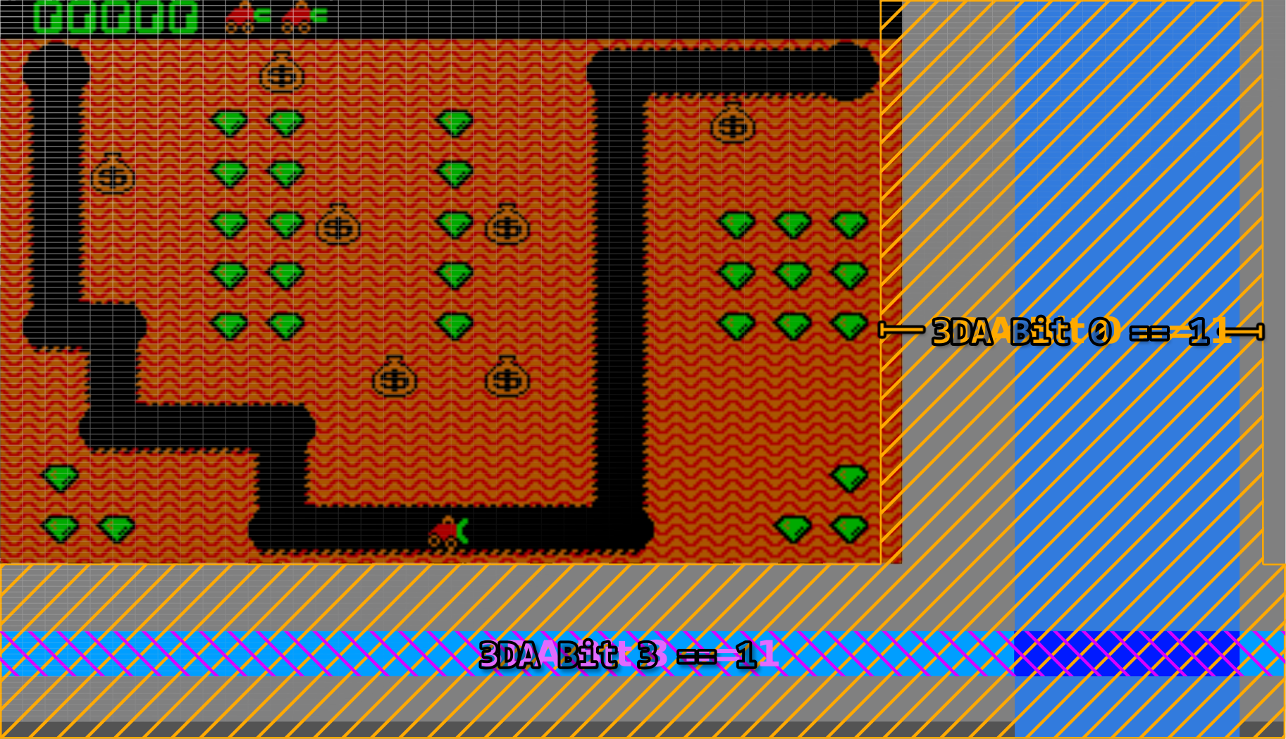
A visualization of the /DE and VR bits in the CGA Status Register (Click to Zoom)
The two other bits in the CGA status register concern themselves with light pen operation.
-
The LPT bit is the state of the light pen strobe trigger. The term trigger can evoke the sense of a physical trigger or button on the light pen, but this is not the case. The light pen trigger is fired when the photodiode within the attached light pen detects light (the strobe) from the CRT raster beam. When this bit is
1, the MC6845’s light pen latch registers should contain the valid approximate position of the light pen. This bit is latched via a flip-flop on the CGA, and will remain set indefinitely unless cleared by writing any value to port3DBh, after which a new strobe trigger may fire and a new light-pen position latched by the MC6845. The strobe trigger may be manually fired without input from the pen by writing to port3DCh. It is possible to crudely determine the current raster position of the display with this method, but it is highly unreliable. Even so, it didn’t stop games like Jungle Hunt from using it to perform mid-frame palette swaps. -
The LPS bit is the immediate state of any switch connected to the light pen header’s switch pin. The light pen switch signal is active-low, explaining why this bit is logically reversed. This is simply the immediate state of any switch present on the light pen - this switch may be at the tip of the pen on high-quality light pens. The switch is typically used for taking actions such as initiating a drawing operation. IBM’s documentation warns us that this signal is not debounced in any way, but a high quality pen should debounce the switch for us.
Text Mode
In text mode, video memory is organized conceptually as a grid of character cells. The dimensions of this grid are directly configured on the CRTC, and are typically 80x25. Each logical cell consists of a pair of bytes in video memory, the first byte being a character code and the second byte being a character attribute.
The character code, combined with the vertical line counter of the CRTC, is used to resolve a byte contained in the CGA’s font ROM representing 8 pixels (or span) of a character glyph. You can see the standard CGA character glyphs below.
CGA Character Glyphs (Standard Font)
| 0 | 1 | 2 | 3 | 4 | 5 | 6 | 7 | 8 | 9 | A | B | C | D | E | F | |
|---|---|---|---|---|---|---|---|---|---|---|---|---|---|---|---|---|
| 0 | ||||||||||||||||
| 1 | ||||||||||||||||
| 2 | ||||||||||||||||
| 3 | ||||||||||||||||
| 4 | ||||||||||||||||
| 5 | ||||||||||||||||
| 6 | ||||||||||||||||
| 7 | ||||||||||||||||
| 8 | ||||||||||||||||
| 9 | ||||||||||||||||
| A | ||||||||||||||||
| B | ||||||||||||||||
| C | ||||||||||||||||
| D | ||||||||||||||||
| E | ||||||||||||||||
| F |
The standard CGA font implements IBM Code Page 437. The vast majority of CGA cards were shipped with this font ROM, however there were variants sold for the international market that contained alternate code pages.1
The CGA ostensibly provides a second “thin” font selectable by a jumper, but on most examples of the IBM CGA this jumper is not populated on the PCB, requiring some soldering to actually utilize. Why IBM changed their mind about making this font user-selectable is up for debate. However, an emulator author can certainly choose to make the font more easily selectable.
A visualization of the character font ROM is shown below, with bytes reversed and wrapping vertically to fit into a square image. The first half of the ROM is dedicated to the MDA’s 8x14 font, each glyph of which is split into two parts. The latter half of the ROM consists of the ‘hidden’ thin font, followed by the standard CGA font.
The MDA/CGA character font ROM (byte-reversed)
The character font ROM is not accessible from the host PC. It can only be read by the CGA itself. int 10h services include routines for drawing text in graphics modes - to accomplish this, a copy of the standard CGA font is present in the IBM PC BIOS as well.
Character Attribute Byte
| Bits | Name | Description |
|---|---|---|
| 0 | FGB | Blue Foreground |
| 1 | FGG | Green Foreground |
| 2 | FGR | Red Foreground |
| 3 | FGI | Foreground Intensity |
| 4 | BGB | Blue Background |
| 5 | BGG | Green Background |
| 6 | BGR | Red Background |
| 7 | BGI / BL | Background Intensity/Blink |
The character attribute byte defines the foreground and background colors the CGA should use when rendering a glyph. The lower four bits provide the color to paint 1 bits which represent the foreground in the raw data from the font ROM. The upper three or four bits provide the color to paint 0 bits which represent the background. Bit 7 is a bit special - the CGA has an optional mode that enables text blinking. When this mode is enabled, bit 7 of the attribute byte controls whether the text blinks or not. This means that only three bits are now available for the background color, so backgrounds are limited to the first 8 “darker” shades when blinking is enabled. See the section on text blinking for more information.
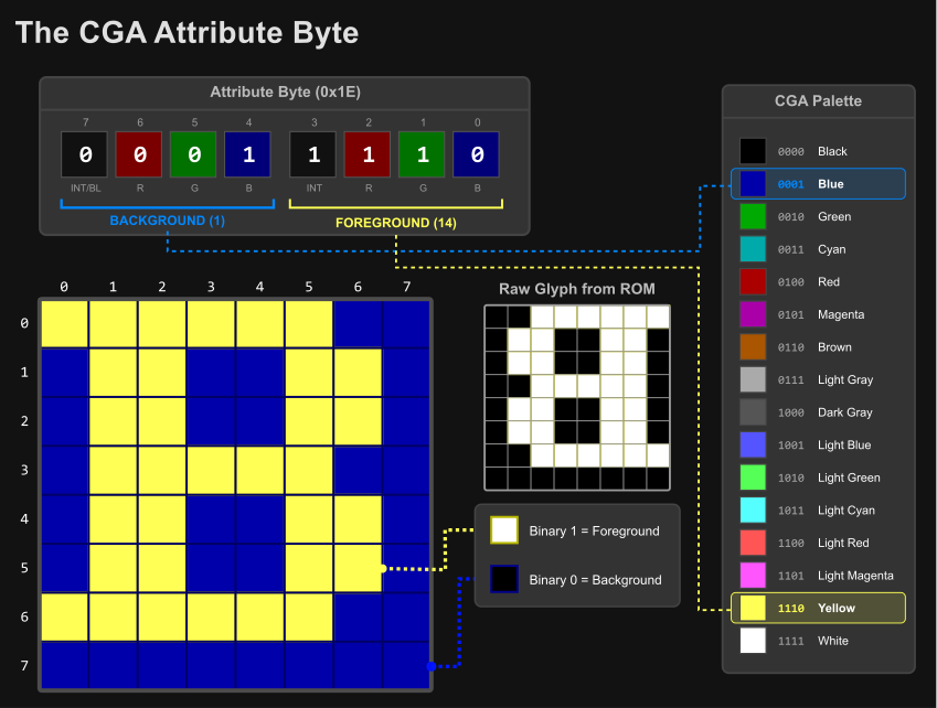
CGA attribute byte visualization
Since each character cell has a character code and attribute byte, each character takes one 16-bit word of memory. Thus it takes 4KiB of memory to display a single 80x25 text mode screen. This means up to four text-mode screens can fit in the CGA’s 16KiB of memory, and a program can switch between each screen by adjusting the CRTC’s start address registers.
When multiple screens can be fit into video memory, they are called video pages. Switching between video pages is referred to as page-switching or page-flipping when used for fast animation, but there are many other uses - a help page could be stored separately from a text editor’s main interface, allowing the program to switch to the help screen and back without having to redraw either page.
Alternatively, a single large screen of up to 80x100 could be stored in memory and the visible 80x25 region panned or scrolled down through it by adjusting the start address registers one row at a time.
Cursor Blinking
The Motorola MC6845 CRTC provides a dedicated CURSOR pin and internally handles blinking at a rate of either 16 (8 frames on, 8 frames off) or 32 fields (16 frames on, 16 frames off). It is possible to configure the MC6845 to disable blinking entirely, which would normally leave a solid, static cursor, and indeed, this is how the IBM PC BIOS configures the MC6845 by default. The cursor blinks anyway, because the CGA card has its own independent blinking logic which is combined with the CURSOR signal from the MC6845.
The CGA’s blink logic is implemented as two 4-bit binary counters, tied to the VSYNC output of the MC6845 as seen below. The \(\overline{\mathrm{CURSOR\_BLINK}}\) signal controls the cursor blinking rate, and will always blink at a rate of 16 fields, equivalent to the normal blink rate of the MC6845. The \(\overline{\mathrm{BLINK}}\) signal controls text blinking and blinks at half the rate due to being output from the next bit of the binary counter chain.

CGA blink signal generation
If the MC6845 is configured for normal blink timings, the CGA’s blink logic will match it perfectly. If the ‘slow’ blink rate is selected, then the CGA’s blink logic and the MC6845’s blink logic will be out of phase; when these signals are effectively AND’d together, the cursor will blink off twice as long as it will blink on:
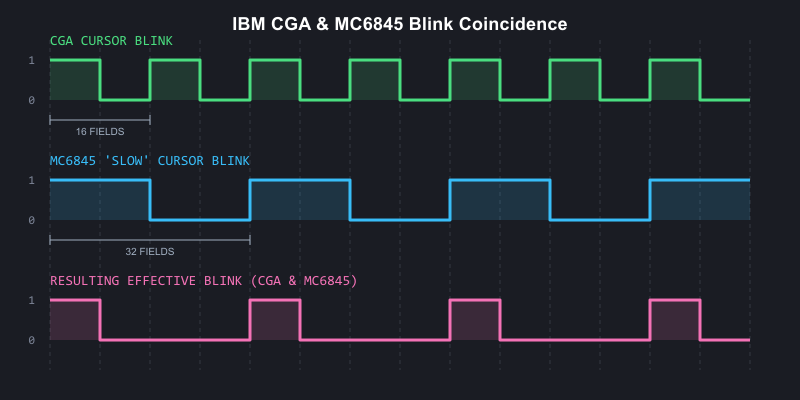
CGA and MC6845 blink coincidence visualized
Besides blinking, the cursor can be disabled a number of ways, or even ‘split’ into two sections. See the MC6845 chapter’s section on cursor tricks.
Text Blinking
Text blinking must first be globally enabled by setting bit 5 of the mode control register. When enabled, bit 7 of each character attribute byte determines whether that character cell will blink.
Blinking text blinks at half the rate of the cursor - 16 frames on, 16 frames off. When text blinks ‘off’, the background attribute is displayed for the entire character cell, allowing for blinking with reverse-video.

Blinking text on the IBM CGA
A subtle, easily-missed detail regarding text blinking on the CGA is that when the MC6845’s cursor signal is active, text blinking is disabled. This only affects the rows of a glyph within the cursor extents. Remember that the MC6845’s cursor is normally configured not to blink. This means that when the CGA’s own blinking disables the cursor, the rows of the glyph subsequently revealed will not blink along with the rest of the glyph.
If the MC6845’s cursor blinking is enabled at either rate, as you can imagine the intended behavior of non-blinking text will be disturbed as the no longer steady CURSOR signal will toggle on and off, periodically enabling and disabling text blinking in the cursor area.
Medium-Resolution Graphics Mode
In the CGA’s 320x200, 4-color graphics mode, pairs of bits (referred to as C0 and C1) are interpreted by the CGA’s color multiplexer more-or-less directly as red and green.
This is an important distinction - the CGA has no traditional graphics palettes as we typically understand them, other than the palette entry used for the background color (when both C0 and C1 are 0). Two bits of each color to be emitted by the CGA are provided from video memory, with the other two bits provided by the PAL_B and PAL_I bits of the color control register.
Medium-resolution graphics mode is enabled by setting the GFX bit in the mode control register.
With the color control register set to its default of 0, we are left with the traditional red-green-brown palette.
| Bytes from video memory are serialized as pairs of bits, C0 and C1. | |
| These bits drive the Red and Green channels. | |
| When both Red and Green are active, yellow is produced... | |
| ...but is converted to brown by the IBM 5153 monitor. |
You can easily see that each of the four traditional ‘palettes’ of the CGA have identical red and green components, differing only in the presence or absence of blue or intensity bits:
Primary Palette (Blue Disabled)
| R | G | B | I | Color | Hex |
|---|---|---|---|---|---|
| 0 | 0 | 0 | 0 | Overscan | |
| 0 | 1 | 0 | 0 | 00AA00 | |
| 1 | 0 | 0 | 0 | AA0000 | |
| 1 | 1 | 0 | 0 | AA5500 |
| R | G | B | I | Color | Hex |
|---|---|---|---|---|---|
| 0 | 0 | 0 | 1 | Overscan | |
| 0 | 1 | 0 | 1 | 55FF55 | |
| 1 | 0 | 0 | 1 | FF5555 | |
| 1 | 1 | 0 | 1 | FFFF55 |
Secondary Palette (Blue Enabled)
| R | G | B | I | Color | Hex |
|---|---|---|---|---|---|
| 0 | 0 | 0 | 0 | Overscan | |
| 0 | 1 | 1 | 0 | 00AAAA | |
| 1 | 0 | 1 | 0 | AA00AA | |
| 1 | 1 | 1 | 0 | AAAAAA |
| R | G | B | I | Color | Hex |
|---|---|---|---|---|---|
| 0 | 0 | 0 | 1 | Overscan | |
| 0 | 1 | 1 | 1 | 55FFFF | |
| 1 | 0 | 1 | 1 | FF55FF | |
| 1 | 1 | 1 | 1 | FFFFFF |
Alternate Palette (Conditional Blue)
There is a third, undocumented palette of cyan, red and white. Many find it to be the most aesthetically pleasing of all the CGA palettes. This particular palette was only implemented to provide better contrast when displaying medium-resolution graphics mode on a monochrome composite display, such as a black-and-white television set. It was not implemented for its color aesthetics, and thus IBM probably didn’t see fit to document it as a distinct palette option. After all, later revisions of the CGA could have always disabled the need for it by adjustments to the composite output circuitry.
The palette is enabled by setting the BW bit in the mode register. The color modification is produced via miscellaneous logic on the CGA that enables the blue video output unless C0 and C1 decode to 10 (red).
| R | G | B | I | Color | Hex |
|---|---|---|---|---|---|
| 0 | 0 | 0 | 0 | Overscan | |
| 0 | 1 | 1 | 0 | 00AAAA | |
| 1 | 0 | 0 | 0 | AA0000 | |
| 1 | 1 | 1 | 0 | AAAAAA |
| R | G | B | I | Color | Hex |
|---|---|---|---|---|---|
| 0 | 0 | 0 | 1 | Overscan | |
| 0 | 1 | 1 | 1 | 55FFFF | |
| 1 | 0 | 0 | 1 | FF5555 | |
| 1 | 1 | 1 | 1 | FFFFFF |
The key point is that medium-resolution graphics mode bit-pairs do not form palette indices in the more typical sense. Instead, they directly form part of an RGBI signal that is completed by the bits in the color control register or alternate external logic.
Graphics Mode Function
If you have read the MC6845 chapter, you may be curious how a text-oriented display controller can be utilized to implement a graphics-oriented mode. The MC6845 still counts out word addresses on the CGA, and for each low-resolution character clock, two bytes are fetched and 8 pixels are emitted. The CGA utilizes the same pair of byte serializers that it uses to serialize the character glyph byte and character attribute byte in text mode, although the color multiplexer is set for input 2.
This is all fine for scanning out individual rows of graphics data, but one immediate issue is present: the vertical total register, vertical displayed register, and vertical character counters of the MC6845 are all only 7 bits. That limits us to a total of 128 logical rows. Medium-resolution graphics mode is 320x200. Clearly, 200 will not fit into 128, so some workaround is needed.
The 8KiB Interleave
IBM came up with a clever solution to this problem, but one that would make programming software for the CGA’s graphics mode fairly cumbersome. In standard graphics modes, rows are set to be two scanlines tall by configuring R9 as 1 (recall this defines the line height of a character row, minus 1). The number of displayed rows, R6, is then set to 100.
This creates 100 logical rows, each two scanlines tall, to give us the desired 200 total visible scanlines. The MC6845 will scan out each logical row twice, with the MC6845’s row counter pin 0, RA0, counting from 0 to 1 for the second scanline.
The memory address line A13 is then exchanged for RA0. This substitution is made when the GFX bit of the mode control is set.
This creates an 8KiB offset in memory for all odd scanlines. Since an extra row-counting bit has been added, we can now define up to 256 scanlines, easily fitting in our 200-line graphics mode, at the cost of an annoying interleaving scheme. Programmers could not simply copy bitmaps or sprites into the CGA’s video memory without taking this interleaving into account.
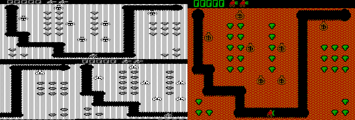
The CGA graphics mode 8KiB offset - video memory visualized side by side with gameplay of 'Digger'
High-Resolution Graphics Mode
This is a 640x200 monochromatic, 1bpp graphics mode. The CGA operates at the low-resolution character clock in this mode, despite the 640 columns of resolution. Each character clock, two bytes from video memory are fetched and 16 pixels are emitted. The color used for drawing 1 bits is the color defined in the color control register.
This is sometimes referred to as the foreground color in this mode, but it is actually still the background color. If that sounds paradoxical, it is explained by the way that this mode is implemented: in high-resolution graphics mode, the CGA’s color multiplexers are set to always draw the border/overscan color. The CGA then rapidly enables and disables the color multiplexers themselves. So in this mode, the foreground is actually the background, and the background is actually just “off.”
You can, of course, leave the color defined in the color control register set to 0, but you will not see anything drawn.
Like medium-resolution graphics mode, an 8KiB offset is created between odd and even scanlines via substitution of A13 with RA0.
High-resolution graphics mode is enabled by setting the GFX and HIRES_GFX bits in the mode control register. Interestingly, the HIRES_GFX bit controls the rapid toggling of the CGA’s color multiplexers, and it is possible to enable this mode at other times - such as in 80-column text mode, and watch as the CGA dutifully toggles the screen on and off as text mode is drawn, leading to a bizarre, striped appearance.
If the B/W bit is set to 0 in this mode, the NTSC color burst is turned on for the composite video output. In this mode, four high-resolution pixels map to a single cycle of the NTSC’s 3.579545MHz color clock, and thus a 16-color video mode is enabled. The exact colors produced are dependent on the value programmed into the color control register.

The black-and-white raw CGA output of Sierra On-line's "Space Quest I" title screen

The same "Space Quest I" title screen as viewed on a color composite monitor
Low-Resolution “Graphics” Mode
Although not actually a graphics mode at all, some games on the PC effectively created a low-resolution graphics mode by setting up a tweaked text mode to display pixel art at an effective resolution of either 80x100 or 160x100.
It is important to differentiate this mode from BIOS video mode 08h which is a true 160x100 graphics mode available only on IBM PCjr and Tandy 1000 systems.
The trick of this mode is to fill video memory with either of two specific CGA character codes:
| Hex | Glyph |
|---|---|
| DD | |
| DE |
Each of these glyphs evenly divides the 8-pixel span of a character cell into half foreground and half background.
Next, the value of R9 on the CRTC is set to 1, making each logical row of character cells two scanlines tall.
Since we can independently control foreground and background colors via character attribute bytes, this essentially creates an all-points-addressable display, with each character cell forming two 4x2 pixel wide ‘pixels’. Updating the screen now involves writing only to the CGA attribute bytes.
Given the CGA’s drastically stretched aspect ratio, these end up displaying as square - as seen below in an aspect-corrected screenshot of the PC shareware title, Round 42:
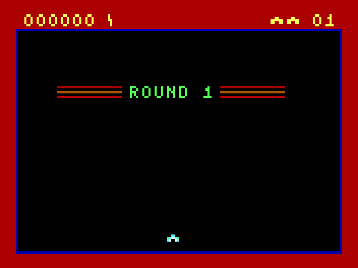
Low-resolution "Graphics" mode in Round 42 by Mike Pooler
Of course, nothing strictly limits you to only using the two convenient ‘split-block’ characters. If we consider using the top two rows of the standard CGA font, many potentially useful patterns can be found:
The top two rows of the IBM CGA code page 437 character set
Several titles by the developer Macrocom utilized this technique, and so it became known in some circles as the “Macrocom Method”, or alternatively, “ANSI from Hell”2.
Here’s an example of how the player character ‘sprite’ in Macrocom’s ICON: Quest for the Ring is built up from standard character glyphs, as seen with varying values for the MC6845’s Maximum Scanline register, R9:

A visualization of the the ASCII-rendered player character in Macrocom's ICON: Quest for the Ring
In 2022, a demo for the PC was released that pushed this technique to its absolute limits: Area 5150. Through many clever additional CRTC tricks, it was able to make it nearly impossible to tell that any of the demo’s effects were actually running in text mode.
| R9==7 | R9==1 |
|---|---|

|
|
For a rather comprehensive review of the various titles that have used a tweaked text-mode over the years, see this excellent post on the blog Nerdly Pleasures.
Light Pen
The IBM CGA provided a header for attaching a light pen. This header supported a pen with active-low strobe and switch signals.
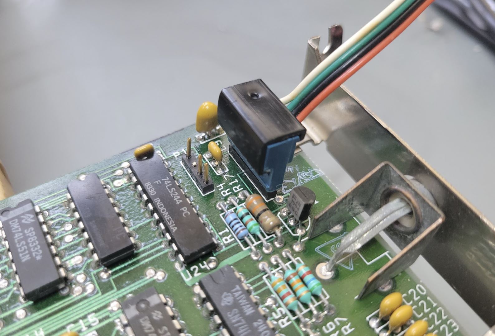
The light pen header (with attached cable) on the IBM CGA card.
The header pinout is:
| Pin | Signal |
|---|---|
| 1 | /LPEN_INPUT |
| 2 | NC |
| 3 | /LPEN_SW |
| 4 | GND |
| 5 | +5V |
| 6 | +12V |
Since the light pen functionality was provided via the MC6845, resolution was limited to character cells. In text mode, this is perfectly acceptable - however it made the light pen less useful in graphics modes. In medium-resolution graphics mode, the horizontal resolution of the pen is limited to 80x200. In high-resolution graphics mode, effective resolution drops to 40x200.
Light pen interface cards were offered by most light pen manufacturers to avoid these limitations. The light pen header on the CGA was rarely used, and very few software titles exist on the PC that natively support the light pen.
Display Timings
Unlike the MDA, the CGA does not have its own crystal. IBM designed the main system crystal of the PC itself around the NTSC display standard, with the apparent intent of simplifying the production of the CGA and other television-compatible peripherals.
The 5150 has a single main system crystal with a frequency of 14.31818MHz. This frequency is exactly four times the NTSC color subcarrier frequency.
The crystal frequency can be expressed as a fraction:
$$f_{crystal} = \frac{315}{22} \text{ MHz} = 14.318181\overline{81} \text{ MHz}$$
The CGA’s output is almost but not quite entirely NTSC-conforming. A real NTSC signal provides two interlaced fields of 262.5 scanlines, whereas the CGA outputs 262 progressive scanlines at approximately 60fps. This 525 vs 524 scanline difference is minor enough for television sets to ignore.
The CGA produces a display field of \(912 \times 262\) or \(238,944\) hdots.
The exact vertical refresh rate of the CGA can be calculated as:
$$f_{refresh} = \frac{14{,}318{,}181}{238{,}944} = 59.92 \text{ Hz}$$
The horizontal retrace rate can be calculated as:
$$f_{hsync} = \frac{14{,}318{,}181}{912} = 15.70 \text{ kHz}$$
This is a significant number in that you will often hear monitors capable of displaying 200-line resolution modes produced by the CGA and EGA video cards described as 15kHZ displays.
Aspect Ratio
The CGA’s display field of 912x262 is quite far from square. The IBM 5153 Color Display has an aspect ratio of approximately 4:3, but this is hardly the final word on the matter - see this VCF forum thread for a surprisingly in-depth discussion of the topic.
The CGA’s aspect ratio is of primary importance when displaying circles - non-circular circles will be immediately obvious to the user. Many monitors had vertical and horizontal adjustment knobs, which a user could use to adjust their display if circles appeared more like ellipses; however, they might find that different adjustments were needed for different software applications that made different assumptions. An emulator author could do worse than to make the effective aspect ratio user-configurable.
A 4:3 aspect ratio applied to a 640-pixel wide image produces the familiar 640x480 resolution. The images in this chapter have all been aspect-corrected to 4:3.
CGA Clocks
The 14.31818MHz clock of the CGA can be used directly as the dot clock, which is the case in the CGA’s high-resolution 80-column text mode. Alternatively, it can be divided by two to produce a 7.159MHz dot clock, which is done in 40-column text mode, and for all of the CGA’s graphics modes. The effect of halving the dot clock effectively doubles the width of each pixel, as the card toggles its RGBI outputs at half the rate, while the monitor continues scanning out at the same rate as always.
The CGA further divides the dot clock by 8 to produce a character clock. In 80-column text mode, this clock runs at 1.79MHz and is called the high-resolution character clock, or hclock. In graphics mode, or 40-column text mode, the CGA accordingly uses the low-resolution character clock or lclock that runs at 895kHz.
When using the hclock, the CGA typically outputs 640 pixels per scanline. When using the lclock, the card typically outputs 320 pixels per scanline, as the effective width of each pixel is doubled since the raster beam continues to scan out the screen at the same rate. The CGA’s high resolution graphics mode is an exception to this, as it has a little trick up its sleeve - it draws by modulating the CGA’s color multiplexers on and off at a rate driven by the original 14MHz dot clock.
Since both the dot and character clocks have the same relationships, it can be useful to discuss the CGA’s effective clock divisor for a given mode. This is fairly easy: for 80-column text mode, the clock divisor is 1 or undivided - for all other modes it is 2.
With either clock, the number of vertical scanlines remains the same, but the horizontal timings programmed into the CRTC must be adjusted to account for the particular dot clock in use.
BIOS Video Modes
The PC BIOS maintains video services via the int 10h service. The first function available, 00, requests that a video mode be set. This led to several standard video mode definitions, the first seven of which, 00h-06h, are modes compatible with the CGA.
| Text / Graphics |
Size | Mono / Color / Grayscale |
Colors | Character Cell | |
|---|---|---|---|---|---|
| 00h | Text | 40x25 chars | Grayscale* | 16 shades | 8x8 |
| 01h | Text | 40x25 chars | Color | 16 colors | 8x8 |
| 02h | Text | 80x25 chars | Grayscale | 16 shades | 8x8 |
| 03h | Text | 80x25 chars | Color | 16 colors | 8x8 |
| 04h | Graphics | 320x200 | Color | 4 colors | 8x2 |
| 05h | Graphics | 320x200 | Grayscale | 4 shades | 8x2 |
| 06h | Graphics | 640x200 | Mono | 1 color | 16x2 |
* Grayscale video will only be displayed on a composite monitor or television set.
CRTC Parameters
For each video mode, the MC6845 CRTC needs to be configured with the correct parameters for registers R0—R9. The standard CRTC parameters are given below.
| Register | Name | Text Mode | Graphics Mode | |||
|---|---|---|---|---|---|---|
| 40 Column | 80 Column | "160x100" | 320x200 | 640x200 | ||
| R0 | HorizontalTotal | 56 | 113 | 113 | 56 | 56 |
| R1 | HorizontalDisplayed | 40 | 80 | 80 | 40 | 40 |
| R2 | HorizontalSyncPosition | 45 | 90 | 90 | 45 | 45 |
| R3 | SyncWidth | 10 | 10 | 10 | 10 | 10 |
| R4 | VerticalTotal | 31 | 31 | 127 | 127 | 127 |
| R5 | VerticalTotalAdjust | 6 | 6 | 6 | 6 | 6 |
| R6 | VerticalDisplayed | 25 | 25 | 100 | 100 | 100 |
| R7 | VerticalSync | 28 | 28 | 112 | 112 | 112 |
| R8 | InterlaceMode | 2 | 2 | 2 | 2 | 2 |
| R9 | MaximumScanLineAddress | 7 | 7 | 1 | 1 | 1 |
Video Memory
The 16KiB of DRAM on the CGA is not expandable. It is also single-ported, meaning that only either the CPU or the CGA can access the video memory at any given time. This is a bit of a problem as the CGA needs to be reading video memory constantly as it rasterizes the screen. We will cover those issues in the next section, Memory Contention.
The 16KiB of video memory is composed of 8 separate 16Kbit DRAM chips, each of which provides a single bit. These bits are organized logically as a 128x128 grid - to address a single bit, a 7-bit column address must be provided followed by a 7-bit row address. The CGA produces these RAS and CAS addresses from the MA pins of the 6845 with some additional manipulation, such as substituting RA0 for A13 in graphics modes.
Memory Contention
The CGA has some circuitry for attempting to arbitrate access to memory between the CPU and the card itself (which IBM refers to, somewhat confusingly, as the CRT). This is done via manipulation of the IO_CH_READY pin of the ISA bus. When this pin is pulled low, any attempts by the CPU to access the CGA’s video memory will stall, with the CPU performing wait states until the pin is released. In this manner the card can guarantee exclusive access to video memory for itself - but only at the slower, 7MHz dot clock. The higher bandwidth requirements of 80-column text mode make this scheme fall apart.
CGA Snow
In 80-column text mode, attempts to access video memory by the CPU while the CGA is rasterizing the active display area will cause a phenomenon called snow - random glitches will briefly appear on the screen, whenever the CGA happens to read data placed on its internal data bus by the CPU while it was attempting to read character glyphs or attribute bytes.
Due to the CGA’s wait state circuitry, even columns are protected from experiencing snow, which only appears on odd columns.
IBM worked around this in BIOS routines that scrolled the screen - such as when you execute the DIR command in DOS - by rapidly disabling and re-enabling the display, causing noticeable flicker. Some people find this flicker more annoying than the snow itself!
Datasheet
- (archive.org) IBM Color Graphics Monitor Adapter
Primary References
- (seasip.info) Colour Graphics Adapter: Notes
- (int10h.org) The IBM 5153’s True CGA Palette and Color Output
- (int10h.org) 8088 MPH Final: Old vs. New CGA (and Other Gory Details)
- (int10h.org) CGA in 1024 Colors - a New Mode: the Illustrated Guide
- (github.org) IBM Colour Graphics Adapter schematics redrawn in KiCad
- (nerdlypleasures.blogspot.com) CGA 16 Color RGB Graphics Modes
Additional Reading
- (reenigne.org) CRTC emulation for MESS
- (martypc.blogspot.com) Exploring CGA Wait States
- (github.com) CGA Accuracy Improvements
Reference Implementations
- (github.com) A digital logic simulation of the IBM CGA card
-
VileR, Name the Non-Standard PC Code Page, August 7, 2024. ↩
-
VileR, CGA in 1024 Colors - a New Mode: the Illustrated Guide, April 2015. ↩
Composite Video
The IBM CGA card supported composite video output via a female RCA connector.
The CGA composite output, an RCA jack, and a monitor's composite input
Composite video is a standard by which luminance, chrominance and synchronization signals such as VSYNC and HSYNC are modulated together on a single wire. Obviously this requires some tradeoffs in image quality. Later video standards, such as S-Video and Component video would improve picture quality by separating these signals onto individual conductors.
An in-depth discussion of the NTSC video display standard is out of scope for this book. Instead, we will discuss the particular aspects of the CGA card’s composite video output that are relevant for emulation.
Warning
The various color diagrams used in this chapter are intended for conceptual visualization only. They are not mathematically rigorous.
The Color Burst
The NTSC broadcast television standard was originally black and white. When color was added to the broadcast signal, it needed to be added in a way that was backwards compatible with black and white television sets. Part of how this was accomplished was by adding a signal called the color burst that only color television sets would understand.
The color burst is a 3.57954MHz reference clock signal emitted during the back porch of a scanline. It is a sine wave about 2.5 microseconds in duration that provides a phase reference for decoding color for that particular scanline. You can see the color burst from an IBM CGA card captured on an oscilloscope below.
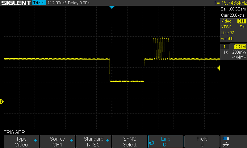
The CGA color burst
Without a color burst signal, the composite video signal for that scanline will be interpreted as luminance only, producing a grayscale picture.
Additive Chrominance
To allow for color to be added to an existing luminance-only signal, we must take the color signal and subtract luminance from it, producing a signal called chrominance. This signal is generally represented by two axes. One possible way to represent a chrominance signal is with a blue axis (with yellow as its complement) and a red axis (with green as its complement). If we call the luminance component Y, these two axes become B-Y and R-Y, since we have subtracted the luminance component from each.
Two proportional terms can be established:
$$ U \propto B’ - Y’ $$
$$ V \propto R’ - Y’ $$
This is the basic derivation of the Y’UV color space.
Phase and the Unit Circle
Color is encoded in a composite signal by comparing the phase offset of the color signal contained within the 3.57954MHz color carrier with the reference phase of the color burst.
We can map YUV colors to the unit circle, assigning an angle to each hue. This produces the YUV color wheel. The color burst represents a reference at 180 on this wheel, mapping to the color yellow. Sometimes you will see the color burst referred to as the yellow burst as a consequence.
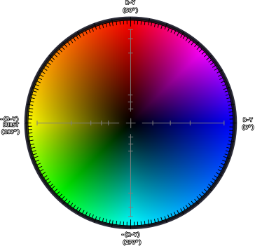
The YUV color wheel (approximate)
YIQ Color Space
Actual NTSC video broadcasts do not directly encode color in the YUV color space. Instead, a rotated color space is used, primarily centered on an axis called I along which most human skin-tones fall. Engineers designing the NTSC video standard could then dedicate more video bandwidth to this axis. I is referred to as the in-phase component, and Q, being 90° from I is called the quadrature component. This is the YIQ color space.
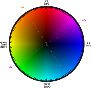
The YUV color wheel with IQ axes (approximate)
The CGA Composite Color Clocks
The CGA produces six square waves representing six unique color clocks. These represent a 3-bit or 8 color “palette”, with black and white not requiring a dedicated clock as they represent a constant low and high logic level, respectively.
An octal 74LS151 multiplexer selects one of the color clocks depending on the internally generated B, G and R color signals. Note that intensity is not used for color clock selection, but contributes to luma instead.
| B | G | R | Clock |
|---|---|---|---|
| 0 | 0 | 0 | Black |
| 1 | 0 | 0 | Blue |
| 0 | 1 | 0 | Green |
| 1 | 1 | 0 | Cyan |
| 0 | 0 | 1 | Red |
| 1 | 0 | 1 | Magenta |
| 0 | 1 | 1 | Yellow |
| 1 | 1 | 1 | White |
Each clock is shifted out of phase in respect to the color burst, which is equivalent to the yellow color clock.
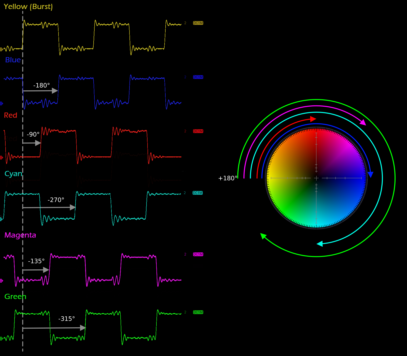
The IBM CGA composite color clocks
This mapping enables a ballpark reproduction of the CGA’s standard graphics palettes on a composite monitor, with the exception that yellow makes a reappearance where the IBM 5153 monitor would have produced brown. The CGA’s infamous magenta also becomes more of a purple shade.
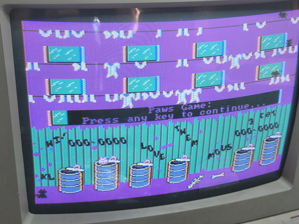
"AlleyCat" by Bill Williams in CGA Composite
In medium-resolution graphics mode, two pixels fit into a single NTSC color cycle. Therefore where high frequency contrast changes occur, color fringing can be observed. These fringes are generally called color artifacts.
Composite color artifacting
Although color artifacting was usually undesirable when displaying graphics designed for RGBI monitors, clever artists could intentionally use pairs of pixels that produce specific artifact colors. If done carefully, the result can be acceptable on both RGBI and composite displays. Notice in this screenshot from The Ancient Art of War at Sea how the stripes in the RGBI graphics produce solid colors on a composite display, notably turning a magenta beard into an actual brown.
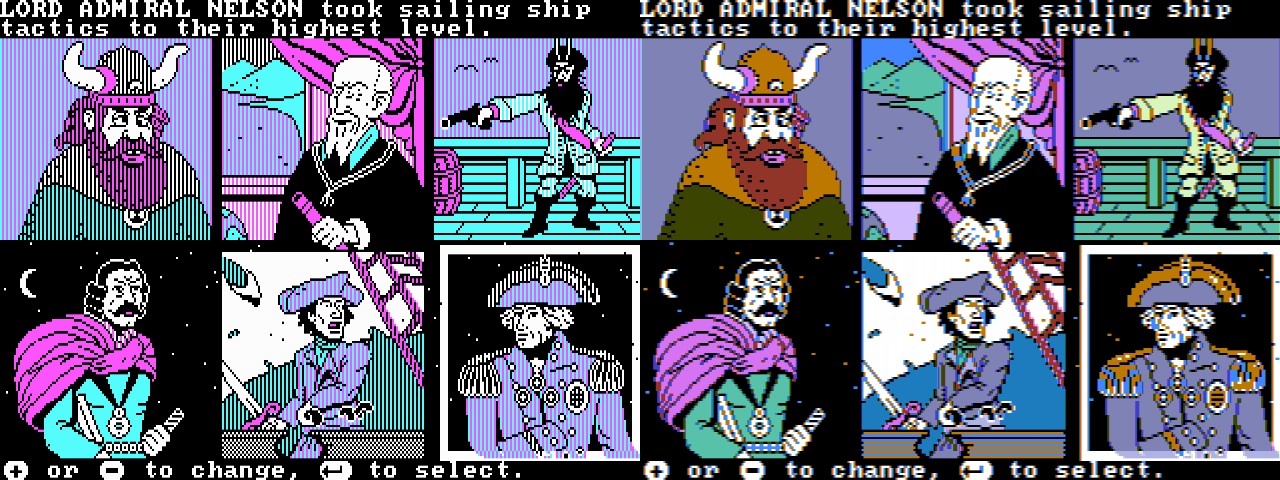
Intentional color artifacting in "The Ancient Art of War at Sea"
Individual pixels will no longer render as white, instead transmuted into a specific color depending on their phase relationship. Notice here how the single-pixel stars in the background of the fourth and six panels become yellow-orange and blue. This particular type of color artifacting will be very familiar to anyone familiar with the Apple II.
Composite and High-Resolution Graphics Mode
Like the Apple II, it is possible to produce a color composite video signal using the CGA’s high-resolution monochrome video mode, relying solely on the effect of color artifacting.
With double the horizontal resolution, four pixels in high-resolution graphics mode fit into a single NTSC color cycle, producing an effective 4-bit or 16-color “palette.” This is not an accident; IBM designed the 14.31818MHz clock of the PC — and thus the dot clock of the IBM CGA — to be exactly four times the frequency of the NTSC color carrier.
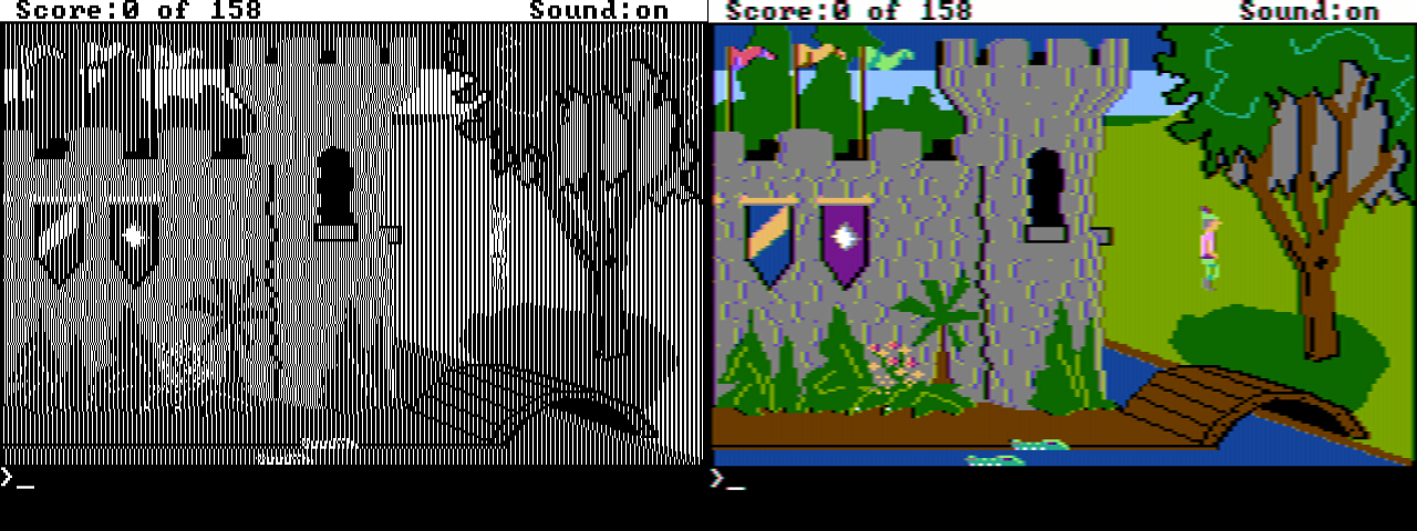
Artifact color in "King's Quest"
Each color cycle represents a traversal of the color wheel. A single lit pixel represents an average of the corresponding quarter of the wheel. Since luminance and chrominance are modulated together, all single-pixel colors are somewhat dark. Additional lit pixels produce brighter, additive colors.

An NTSC color cycle, with quarter-wheel averages

Single-pixel artifact colors, mapped to color cycles
If we zoom in to the upper-left of the King’s Quest screenshot with two of the pennants in view, we can analyze how the high-resolution black and white graphics become color.
Black and white graphics in "King's Quest"
Each pixel or run of pixels maps to the corresponding average of the color wheel which the pixels cover, with the total luma a function of how many pixels are lit within a color cycle.
Color cycle mappings in "King's Quest"
The luminance of the image is sampled at a lower frequency than chrominance; therefore regular patterns of pixels produce solid colors. Note that due to the coupling of luminance and chrominance it is impossible to change between certain colors without a corresponding luminance fringe due to the change in color phase inducing an increase or decrease in immediate luminance. This is most visible at the left edge of the green tree canopy where the shift from blue to green moves 90°.

Composite artifact color in "King's Quest"
The High-Resolution CGA Composite Color Gamut
The following references assume that the foreground color of the CGA’s high-resolution graphics mode is set to bright white. Any other color will produce one of 14 alternate composite palettes. However, almost every title that uses artifact color graphics uses bright white in practice.
The combination of any four lit pixels produces \(2^{4}\) or 16 possible colors. If each pattern is repeated along 4-pixel color cycles, they produce solid bars of color.
Composite artifact color in high-resolution graphics mode (NewRisingSun)
| B0 | B1 | B2 | B3 | Color | Hex |
|---|---|---|---|---|---|
| 0 | 0 | 0 | 0 | 000000 | |
| 0 | 0 | 0 | 1 | 00680C | |
| 0 | 0 | 1 | 0 | 212BBD | |
| 0 | 0 | 1 | 1 | 0D9ED5 | |
| 0 | 1 | 0 | 0 | 85096C | |
| 0 | 1 | 0 | 1 | 757376 | |
| 0 | 1 | 1 | 0 | AF36FF | |
| 0 | 1 | 1 | 1 | 9BA9FF | |
| 1 | 0 | 0 | 0 | 514700 | |
| 1 | 0 | 0 | 1 | 42BD00 | |
| 1 | 0 | 1 | 0 | 707470 | |
| 1 | 0 | 1 | 1 | 5DF47A | |
| 1 | 1 | 0 | 0 | E5541D | |
| 1 | 1 | 0 | 1 | D7CB19 | |
| 1 | 1 | 1 | 0 | FF81F2 | |
| 1 | 1 | 1 | 1 | FDFFFC |
The composite colors can alternatively be sorted by hue:
| B0 | B1 | B2 | B3 | Color | Hex |
|---|---|---|---|---|---|
| 0 | 0 | 0 | 1 | 00680C | |
| 1 | 0 | 0 | 1 | 42BD00 | |
| 1 | 0 | 1 | 1 | 5DF47A | |
| 0 | 0 | 1 | 0 | 212BBD | |
| 0 | 0 | 1 | 1 | 0D9ED5 | |
| 0 | 1 | 1 | 1 | 9BA9FF | |
| 0 | 1 | 0 | 0 | 85096C | |
| 0 | 1 | 1 | 0 | AF36FF | |
| 1 | 1 | 1 | 0 | FF81F2 | |
| 1 | 0 | 0 | 0 | 514700 | |
| 1 | 1 | 0 | 0 | E5541D | |
| 1 | 1 | 0 | 1 | D7CB19 |
Or by hue and luminance:
| B0 | B1 | B2 | B3 | Color | Hex | B0 | B1 | B2 | B3 | Color | Hex | B0 | B1 | B2 | B3 | Color | Hex |
|---|---|---|---|---|---|---|---|---|---|---|---|---|---|---|---|---|---|
| 0 | 0 | 0 | 1 | 00680C | 1 | 0 | 0 | 1 | 42BD00 | 1 | 0 | 1 | 1 | 5DF47A | |||
| 0 | 0 | 1 | 0 | 212BBD | 0 | 0 | 1 | 1 | 0D9ED5 | 0 | 1 | 1 | 1 | 9BA9FF | |||
| 0 | 1 | 0 | 0 | 85096C | 0 | 1 | 1 | 0 | AF36FF | 1 | 1 | 1 | 0 | FF81F2 | |||
| 1 | 0 | 0 | 0 | 514700 | 1 | 1 | 0 | 0 | E5541D | 1 | 1 | 0 | 1 | D7CB19 |
Note
It might be tempting to make a simple 16-color LUT and emit chunky 4-pixel-wide spans of color, however this will not produce a satisfactory result. The luminance signal must be sampled independently and combined with chrominance information to reproduce the composite output’s full perceptual horizontal resolution.
80-Column Text Mode Caveats
In 80-column text mode, the IBM CGA card disables the color burst, at least when using the standard CRTC register values. The cause of this is U64, a 74LS164 8-bit shift register that generates the trigger for the color burst generation circuitry. It requires 7 lclocks to fire. In both 80-column and 40-column text mode, the CRTC’s HSYNC width register R3 is set to 10. Given the faster character clock in 80-column text mode, this equates to only 5 lclocks and thus the color burst never triggers.
This is actually a good thing for most users, as it turns 80-column text mode from what would be a smeary, technicolor mess into a fairly usable grayscale signal. Clones of the IBM CGA did not always behave in a similar manner, so switching into 40-column text mode was a useful workaround for a readable DOS prompt.
It is possible to re-enable the color burst in 80-column text mode by adjusting the value of R3. On a Motorola MC6845 setting R3 to 0 will produce an effective value of 16, which is sufficient for the color burst to trigger.
Old vs New CGA
At some point, IBM redesigned the CGA’s composite output stage to make the RGBI color outputs contribute more to the luminance signal. Cards made before this change are called old style CGA cards, while cards made after the change are called new style cards. The new style redesign improved the ability to discriminate individual colors on grayscale composite monitors, an important feature intended to support IBM’s Model 5155 Portable Computer1. Unfortunately, this means that any composite conversion code must now be able to handle both models for accuracy.
8088 MPH
Perhaps the most infamous use of CGA composite artifact color is the PC demo 8088 MPH.

The 8088 MPH Title Screen
8088 MPH's 1024 Color Mode
It would be difficult to explain the tricks used in this demo better than VileR — one of the demo’s creators — already did. Check out his excellent series of two blog articles starting here.
Simulation vs Sampling
The exact characteristics of the CGA’s composite output cannot be accurately reproduced with a purely digital simulation. The colors are slightly modified by the analog characteristics of the circuit, starting with the output of the composite color multiplexer itself.
Reenigne took a statistical approach and sampled the output of both the old and new-style CGA cards using a video capture card to produce a highly accurate composite rendering algorithm - see the VOGONS link in Reference Implementations for a link to the original patch for DOSBox. Nearly all prominent PC emulators now use reenigne’s code for CGA composite rendering. It is fast and hard to beat for quality.
Primary References
- (int10h.org) CGA in 1024 Colors - a New Mode: the Illustrated Guide
- (int10h.org) 8088 MPH Final: Old vs. New CGA (and Other Gory Details)
- (reenigne.org) CRTC Emulation for MESS
- (nerdlypleasures.blogspot.com) IBM PC Color Composite Graphics
Reference Implementations
- (vogons.org) CGA Composite Mode under DOSBOX (Committed r3804)
- (github.org) CGA Artifact Color
Inline References
-
Bill Machrone, “Inside the PC Portable,” PC Magazine, vol. 3, no. 10, May 29, 1984, pp. 117–119. Internet Archive ↩
Keyboard
The IBM 5150 and 5160 originally used an 83-key IBM “Model F” keyboard1, IBM Part #1501100 (Part #1501105 in the UK2).
Later revisions of the BIOS ROM for the IBM 5160 contained support for the 101-key Enhanced Keyboard3. This keyboard introduced multi-byte scancodes, which required large changes in the keyboard handling code of the BIOS to accommodate.
IBM changed the keyboard protocol with the IBM 5170 AT, making everyone buy new keyboards. Therefore, keyboards of this era are often described as speaking either the “XT” or “AT” protocol. Some keyboards were made that could switch between both, and adapters were (and are) available.
The 83-key keyboard layout is missing many of the keys that we take for granted on modern keyboard layouts. Unlike modern keyboards, the function keys are arranged in a block on the left side.
Figure 1.1: IBM PC 83-key Model F Keyboard Layout with scancodes (Click to zoom)
Keyboard Operation
The keyboard communicates with the PC by sending scancodes when a key is pressed or released. On the original 83-key keyboard, each key produces a pair of single-byte scancodes, one when pressed, called the make scancode, and one when released called the break scancode. The make scancodes are typically the values provided in scancode tables, and can be seen in the figure above. Break scancodes are calculated by taking the make scancode and setting the MSB to 1.
Since keyboard operation is event-driven, if the host computer were ever to miss processing a ‘key-up’ scancode, this would cause the phenomenon of a “stuck key,” something most PC users have experienced at one point.
Inside the Model F keyboard is an Intel 8048 microcontroller that is responsible for scanning the internal capacitive key matrix and converting key-presses (and releases) into scancodes to send to the host PC. On early versions of the Model F, the 8048 could be reset directly through the RESET pin on the keyboard DIN connector. Later versions of the Model F disconnected this RESET line and the 8048 is no longer externally resettable, except perhaps by unplugging the keyboard.
The 8048 has burned-in program ROM and a small amount of onboard RAM, in which it keeps a 16-byte scancode FIFO buffer. Scancodes are placed into this buffer as they are detected from the keyboard matrix, and read out as they are sent to the host.
Note
It is important that you buffer scancodes in your emulator - a fast typist can generate scancodes very rapidly - consider how quickly scancodes may be produced in the event that multiple keys are pressed and released at once. It is generally insufficient to deliver one scancode per frame.
The keyboard is a serial device, and the keyboard port is a specialized serial port. The exact electrical details of the keyboard port are not crucially important to emulating the keyboard, except for the operation of the clock pin.
The clock pin is normally pulled up by the motherboard. Both the computer and the keyboard can pull the clock line low - the motherboard has a special driver for this, whereas the keyboard relies on an open-drain output pin.
Setting bit 6 of the 8255 PPI’s Port B register to 0 will result in the motherboard pulling the keyboard clock line low. The keyboard can detect this condition. When held in this state for approximately 20ms, the 8048 will perform a keyboard self-test. When the clock line is released by writing 1 to PPI Port B bit 6, the keyboard will send the special scancode 0xAA about 6-8ms later. If the keyboard internally detects a physically stuck key, it will send the scancode of that key 10ms after sending 0xAA.4.

Figure 1.2: Keyboard reset byte 0xAA timing trace (Click to zoom)
If you fail to emulate sending the reset scancode 0xAA at the appropriate time, the BIOS will emit a POST error code 301.
It is important to note that the ‘clock’ line does not actually clock the 8048 MCU itself. The keyboard data and clock lines are simply connected to specialized I/O pins on the 8048 that allow it to monitor the voltage level of each line, or pull the line to ground.
The 8048 is operationally clocked via an internal oscillator, the speed of which is set in via an LC resonant circuit that configures it for approximately 5MHz. The 8048 is not quite that fast in actual operation due to an internal clock divisor of 15.
Typematic Repeat
Most computer users are familiar with what typically happens when a key on the keyboard is held down: after a short delay, the keyboard will begin repeating the keypress automatically.
IBM called this feature typematic repeat on the Model F. When a key is held down, it will start to repeat after approximately 500ms at a rate of approximately 11 characters per second. Both the make and break scancodes are sent for each repeat.
It is possible to simply pass through the host’s typematic repeat to your emulator, but I recommend handling it yourself, as it gives you better control over the rate (which might otherwise be too fast).
There are some subtleties to typematic repeat operation:
- If more than one key is held down, only the last key will repeat.
- Repeat will stop when a key is released, even if other keys remain held down.
The IBM BIOS keyboard routines will filter typematic events for Ctrl, Shift, Alt, Num Lock, Scroll Lock, Caps Lock, and Insert. If the default BIOS keyboard routines are used by an application that does not process keyboard events fast enough, it is likely that holding down a key will fill the BIOS keyboard buffer and result in several angry beeps from the PC speaker.
The Keyboard Interface
Serial data from the keyboard is first read into a shift register on the motherboard, then ultimately read out in a parallel fashion via the 8255 PPI’s Port A. See the chapter on the IBM PC/XT Keyboard Interface for more details.
SDL Scancode Table
If you happen to be using SDL for your emulator, here’s a table of SDL keycode definitions to IBM scancodes:
| SDL Key | Scancode (hex) |
|---|---|
| SDLK_A | 1E |
| SDLK_B | 30 |
| SDLK_C | 2E |
| SDLK_D | 20 |
| SDLK_E | 12 |
| SDLK_F | 21 |
| SDLK_G | 22 |
| SDLK_H | 23 |
| SDLK_I | 17 |
| SDLK_J | 24 |
| SDLK_K | 25 |
| SDLK_L | 26 |
| SDLK_M | 32 |
| SDLK_N | 31 |
| SDLK_O | 18 |
| SDLK_P | 19 |
| SDLK_Q | 10 |
| SDLK_R | 13 |
| SDLK_S | 1F |
| SDLK_T | 14 |
| SDLK_U | 16 |
| SDLK_V | 2F |
| SDLK_W | 11 |
| SDLK_X | 2D |
| SDLK_Y | 15 |
| SDLK_Z | 2C |
| SDLK_1 | 02 |
| SDLK_2 | 03 |
| SDLK_3 | 04 |
| SDLK_4 | 05 |
| SDLK_5 | 06 |
| SDLK_6 | 07 |
| SDLK_7 | 08 |
| SDLK_8 | 09 |
| SDLK_9 | 0A |
| SDLK_0 | 0B |
| SDLK_RETURN | 1C |
| SDLK_ESCAPE | 01 |
| SDLK_BACKSPACE | 0E |
| SDLK_TAB | 0F |
| SDLK_SPACE | 39 |
| SDLK_MINUS | 0C |
| SDLK_EQUALS | 0D |
| SDLK_LEFTBRACKET | 1A |
| SDLK_RIGHTBRACKET | 1B |
| SDLK_BACKSLASH | 2B |
| SDLK_SEMICOLON | 27 |
| SDLK_APOSTROPHE | 28 |
| SDLK_COMMA | 33 |
| SDLK_PERIOD | 34 |
| SDLK_SLASH | 35 |
| SDLK_GRAVE | 29 |
| SDLK_LSHIFT | 2A |
| SDLK_RSHIFT | 36 |
| SDLK_LCTRL | 1D |
| SDLK_RCTRL | 1D |
| SDLK_LALT | 38 |
| SDLK_RALT | 38 |
| SDLK_CAPSLOCK | 3A |
| SDLK_F1 | 3B |
| SDLK_F2 | 3C |
| SDLK_F3 | 3D |
| SDLK_F4 | 3E |
| SDLK_F5 | 3F |
| SDLK_F6 | 40 |
| SDLK_F7 | 41 |
| SDLK_F8 | 42 |
| SDLK_F9 | 43 |
| SDLK_F10 | 44 |
| SDLK_F11 | 57 |
| SDLK_F12 | 58 |
| SDLK_UP | 48 |
| SDLK_DOWN | 50 |
| SDLK_LEFT | 4B |
| SDLK_RIGHT | 4D |
| SDLK_INSERT | 52 |
| SDLK_DELETE | 53 |
| SDLK_HOME | 47 |
| SDLK_END | 4F |
| SDLK_PAGEUP | 49 |
| SDLK_PAGEDOWN | 51 |
| SDLK_KP_1 | 4F |
| SDLK_KP_2 | 50 |
| SDLK_KP_3 | 51 |
| SDLK_KP_4 | 4B |
| SDLK_KP_5 | 4C |
| SDLK_KP_6 | 4D |
| SDLK_KP_7 | 47 |
| SDLK_KP_8 | 48 |
| SDLK_KP_9 | 49 |
| SDLK_KP_0 | 52 |
| SDLK_KP_PLUS | 4E |
| SDLK_KP_MINUS | 4A |
| SDLK_KP_PERIOD | 53 |
| SDLK_KP_ENTER | 1C |
| SDLK_KP_DIVIDE | 35 |
| SDLK_KP_MULTIPLY | 37 |
| SDLK_KP_EQUALS | 0D |
Primary References
Citations
-
wikipedia.org Model F keyboard. ↩
-
seasip.info The IBM 1501105 Keyboard ↩
-
minuszerodegrees.net IBM 5160 - Keyboards ↩
-
minuszerodegrees.net 5160 Keyboard Startup ↩

The Parallel Port
The IBM Printer Adapter
The term parallel is in contrast to serial. The parallel port provides an 8-bit bidirectional data path, whereas a bidirectional serial connection typically uses a pair of wires, transferring one bit at a time.
The PC parallel port was typically used to interface with a printer, but over the years a number of other devices utilized the parallel port, from storage devices to sound generators. Hobbyists could use the parallel port to connect to breadboards and control various projects.
When connecting to a printer, a printer cable was typically used with a male DB-25 connector on one end and a Centronics connector on the other, named after the Centronics Data Computer Corporation.
The parallel port can be implemented entirely with off-the-shelf 74-series logic chips and a few discrete components. IBM sold a dedicated ISA card called the IBM Printer Adapter that provided a single parallel port. A parallel port was often included as a ‘bonus accessory’ on other cards, such as the Monochrome Display Adapter, various multifunction adapters, and several other third-party video cards.
At a Glance
| Item | Description |
|---|---|
| Typical LPT1 base address | 378h (or 3BCh on the MDA*) |
| Typical LPT2 base address | 278h |
| Data register | Base address + 0 |
| Status register | Base address + 1 |
| Control register | Base address + 2 |
| Interrupts | Usually IRQ7 for LPT1, IRQ5 for LPT2 |
| DMA | None |
Note
*There is no fixed address for LPT1, 2 and 3. Device names are assigned to ports discovered in the order
3BCh,378h,278h.
Registers
The Parallel Data Register
| Bits | Name | Description |
|---|---|---|
| 0:7 | DATA | Data byte |
The Parallel Status Register
| Bits | Name | Description |
|---|---|---|
| 0:2 | Unused | Unused |
| 3 | ERROR | 0: The printer has encountered an error condition. 1: The printer reports no current error condition. |
| 4 | SLCT | 0: The printer has not been selected (Printer offline) 1: The printer has been selected (Select/Online button pressed) |
| 5 | PE | 0: The printer reports it has paper. 1: The printer reports it is out of paper. |
| 6 | ACK | 0: The printer has acknowledged the last character and is ready to receive another. 1: The printer is processing (busy). |
| 7 | BUSY | 0: The printer is busy and cannot accept data. 1: The printer is not busy and can receive data. |
The Parallel Control Register
| Bits | Name | Description |
|---|---|---|
| 0 | STR | Data clock strobe to feed data into the printer. |
| 1 | ALF | 0: Do not line-feed automatically. 1: Line-feed automatically. |
| 2 | INIT | 0: Initialize the printer. 1: Do nothing. |
| 3 | SLCT_IN | 0: Leave printer unselected. 1: Select the printer. |
| 4 | IRQEN | 0: Disable interrupts. 1: Enable interrupts triggered by a rising edge of the pin. |
| 5:7 | Unused | Unused |
Datasheet
- (archive.org) IBM Printer Adapter
- (archive.org) IBM Serial/Parallel Adapter
The Game Port
The IBM Game Control Adapter
The IBM Game Control Adapter implements a game port, supporting up to four buttons and four analog axes. In the early days of the PC, joysticks typically had two axes (one stick) and two buttons. Later on, gamepads with four buttons emerged, such as the Gravis PC Gamepad.
Eventually, joystick makers employed various schemes to support more than four buttons and inputs such as hat switches.
This included implementing bespoke digital protocols on top of the existing game port wiring. Digital joystick protocols will not be discussed here.
At a Glance
| Item | Description |
|---|---|
| I/O address | 201h |
| Interrupts | None |
| DMA | None |
Game Port Operation
The pinout of the game port itself presents a challenge: the position of each axis must somehow be read with a single wire.
To do so, each axis of a joystick is connected to a potentiometer. A capacitor on the game port card and the potentiometer within the joystick form an RC timing network connected to one of four monostable timers on an NE558N quad-timer chip. This creates a one-shot timing pulse of a duration given by the following formula:
$$ T(\mu\mathrm{s}) = 24.2\mu\mathrm{s} + 0.011r\ \mu\mathrm{s} $$
To read the axis positions, first port 201h must be written to in order to trigger the four timers. This will cause bits 0-3 of 201h to read high. Port 201h must then be polled repeatedly until one axis bit changes from 1 to 0. At this point, the elapsed time T (in microseconds) can provide the resistance value for that axis:
$$ r(\Omega) = \frac{T(\mu\mathrm{s}) - 24.2}{0.011} $$
The measured resistance value can be normalized to the range [0.0-1.0] by dividing by the maximum resistance. The potentiometers in the joystick typically have a range of 0 to 100kΩ. An emulator can simulate an ideal joystick with a perfect, linear response within this full range. Real joysticks were imperfect, and so many applications that used a joystick had a calibration routine where the user was asked to move the stick to the maximum extent of each axis before pressing a button. In this way the effective range of the potentiometer could be determined.
When the stick of a joystick is auto-centered, the stick is said to be in its neutral position. In the neutral position, the joystick may not read at the exact center of its range. Some joysticks included trim controls that could be used to adjust the center position until it read correctly. A robust joystick calibration routine should also capture the neutral position to account for any off-center readings.
Without sufficient calibration, a phenomenon known as drift may occur where an unintended directional input is produced while the joystick remains in the neutral position.
One way for a programmer to address drift was to establish a dead zone, a square region or radius within which any calculated stick position is snapped to the ideal neutral position.
Reading Buttons
The immediate state of the four buttons can be read out at any time, as active-low inputs.
The Game Port Status Register
| Bits | Name | Description |
|---|---|---|
| 0 | A-X | Joystick A X-coordinate one-shot output. 0: Timing pulse ended 1: One-shot fired / timing pulse active |
| 1 | A-Y | Joystick A Y-coordinate one-shot output. 0: Timing pulse ended 1: One-shot fired / timing pulse active |
| 2 | B-X | Joystick B X-coordinate one-shot output. 0: Timing pulse ended 1: One-shot fired / timing pulse active |
| 3 | B-Y | Joystick B Y-coordinate one-shot output. 0: Timing pulse ended 1: One-shot fired / timing pulse active |
| 4 | A1 | Joystick A button 1. 0: Pressed 1: Open / not pressed |
| 5 | A2 | Joystick A button 2. 0: Pressed 1: Open / not pressed |
| 6 | B1 | Joystick B button 1. 0: Pressed 1: Open / not pressed |
| 7 | B2 | Joystick B button 2. 0: Pressed 1: Open / not pressed |
Typical Joystick
A typical joystick of the original PC era would have a single stick, and one or two buttons. The IBM PCjr joystick pictured below was a rebadged Kraft joystick that could also be purchased for a standard PC game port. This joystick, like many others, can be converted per-axis from auto-centering to free movement, something probably only useful for flight-simulator games.
The IBM Joystick
Typical Game Pad
Game pads typically had a directional pad (or D-pad) that acted in a digital fashion, snapping to the farthest extent of either of two joystick axes when a direction was pressed. Directional pads were more suitable for fast action games and were the primary means of directional input for popular home video game consoles such as the NES.
The Gravis PC GamePad shown here could be switched between left and right-hand operation, as well as between two and four-button mode. Two gamepads could only be used at the same time in two-button mode.
The Gravis PC Gamepad
Hat Switches
A hat switch is a multidirectional input present on some joysticks that is typically operated with the user’s thumb. It typically allows four directions of input, and can be useful in flight simulators for changing camera views or navigating through menus.
Two separate and incompatible techniques emerged for encoding hat switch input.
Thrustmaster Hat Switch Input
The first came from the joystick manufacturer Thrustmaster to support the hat switch on the Thrustmaster FCS.
The four positions of the hat switch were encoded as five specific resistance values measured on the single B-Y axis.
| Value | Hat position |
|---|---|
| 0.2 kΩ | Up |
| 20 kΩ | Right |
| 40 kΩ | Down |
| 60 kΩ | Left |
| 82 kΩ | Center |
This implies interpreting resistance bands as follows:
| Low | High | Center Fraction | Hat position |
|---|---|---|---|
| 0 kΩ | 10 kΩ | 1/8 | Up |
| 10 kΩ | 31 kΩ | 3/8 | Right |
| 31 kΩ | 51 kΩ | 5/8 | Down |
| 51 kΩ | 72 kΩ | 7/8 | Left |
| 72 kΩ | ~ | Center |
Note
Various references conflict on the ordering of these inputs. This is the ordering used by the Linux analog joystick driver, and several modern microcontroller projects.
CH Products Hat Switch Input
The competing hat switch encoding standard was from CH Products. In this scheme, multiple inputs or chords of the standard four buttons encode the hat switch position. The downside of this scheme is losing the ability to register more than one simultaneous button press during normal input.
| Button A1 | Button A2 | Button B1 | Button B2 | Hat position |
|---|---|---|---|---|
| 0 | 0 | 1 | 0 | Right |
| 0 | 0 | 1 | 1 | Left |
| 0 | 0 | 0 | 0 | Up |
| 0 | 0 | 0 | 1 | Down |
If multiple buttons are pressed, only a single button will register, based on the lowest priority number.
| Button | Priority |
|---|---|
| A1 | 1 |
| A2 | 2 |
| B1 | 3 |
| B2 | 4 |
Radial Remapping
Modern analog sticks are typically circular, producing coordinate pairs in the unit circle:
$$ x^2 + y^2 \leq 1 $$
Traditional joysticks typically allowed the full range of each axis independently. This can cause problems when calibrating a joystick via diagonal inputs with a modern gamepad. It may be useful to translate radial coordinates to square ones:
$$ r = \sqrt{x^2 + y^2}, \qquad m = \max\left(|x|, |y|\right), \qquad (x’, y’) = \frac{r}{m}(x, y) $$
This produces the following remapping:
Game Port Evolution
The game port didn’t exist for long as a standalone card, although several companies produced their own versions, sometimes with a trim adjustment knob for better calibration. Game ports instead started to appear on many multifunction cards like the AST SixPakPlus. Eventually, the game port would migrate almost entirely to PC sound cards such as the SoundBlaster, where the port also served a secondary role as a MIDI port.
Utilities
- (www.oldskool.org) JOYCALIB is an excellent joystick calibration utility made by Trixter. It can be very useful for testing your game port and joystick emulation.
Datasheet
- (archive.org) The IBM Game Control Adapter
Primary References
- (atrey.karlin.mff.cuni.cz @ archive.org) Vojtech Pavlik’s Joytic Specifications
- (epanorma.net) Joysticks and other game controllers
- (davenunez.wordpress.com @ archive.org) Reading hat switches on PC gameport joysticks
- (nerdlypleasures.blogspot.com) Three Flight Simulator Joysticks for DOS
- (github.com) /drivers/input/joystick/analog.c
Electronics Concepts
You don’t need to have a degree in Electronics Engineering to emulate the PC, but from time to time certain electrical concepts do come up, especially when discussing the schematics for the system. A complete overview of basic electronics theory is out of scope, but here are some refresher concepts.
Resistance
Resistance is a measurement of opposition to the flow of electric current. If you viewed electric current was water flowing through a flexible hose, pinching the hose would be analogous to increasing resistance. Resistance is often expressed as the symbol R, and the SI unit for resistance is the ohm (Ω). A common component with a specified resistance in ohms is called a resistor.
On the PC, resistors appear as small, cylindrical objects with colored stripes. These stripes specify the resistance value. You can use a resistor calculator to determine the exact value from the color codes.
Capacitance
Capacitance is a measure of the ability to store electric charge. Capacitance is often expressed as the symbol C and its SI unit is the farad (F). A common component with a specified capacitance in farads is called a capacitor. Capacitors on the original PC are typically used for power filtering - including the PC’s infamous tantalum capacitors with a penchant for tiny explosions. Capacitors are also fundamental to the operation of the PC’s game port and joysticks.
Inductance
Inductance is a property of a conductor that resists changes in current flow. Flowing current in a conductor generates a magnetic field. Changes in current through the conductor create or induce a corresponding voltage that opposes this change. In the PC, this is typically encountered in the operation of the speaker, and the deflection yoke in the monitor. The principle of inductance and electromagnetism are also central to the operation of relays and electric motors.
Impedance
Impedance is the effective opposition a circuit presents to current in an AC or time-varying signal. Digital circuits are powered by DC, but their fast signal transitions behave like time-varying signals, so impedance effects still matter. Impedance is often expressed as the symbol Z. It’s SI unit is also the ohm (Ω), but values for impedance can be given as complex numbers. Don’t let that scare you - discussion of impedance here will be limited to broad concepts.
Impedance typically comes up in context of characterizing a chip’s output pins. In digital logic, typically a signal can be either logically high (a state equivalent to binary 1), or logically low (a state equivalent to binary 0). However, a third state is possible, which is “neither 1 nor 0.” In this state, the output pin has a very high impedance, or Z value. Thus this state is often called High-Z. In this state the pin will not source or sink much current, if any. It is almost as if the pin is disconnected from the circuit.
An output pin that can enter a high-impedance or high-Z state is said to be a tri-state output. The main purpose of a tri-state output is to enable multiple bus drivers to attach to the same wire without electrical complications. Consider a video card with on-board video memory - its bus drivers must allow the CPU to read and write to this memory, but the video card needs to do so as well. The Output Enable () pin on a bus driver chip can allow one bus driver to ‘detach’ from the bus allowing the other access.
Impedance is not always a desirable phenomenon. Long traces with high speed clocks can experience ringing or reflections due to impedance mismatch. The actual details are not salient to emulation discussions, but for this reason termination resistors are often employed on bus and clock lines to compensate for impedance mismatches and reduce undesirable effects.
Terminators were employed with many early electrical communications standards. Termination packs often needed to be installed in floppy drives, and special termination connectors attached to SCSI device chains and the ends of coaxial Ethernet cables.
Push-Pull Output Drivers
A chip’s pins are typically some kind of input pin or output pin, or both - in which case the pin is said to be bidirectional.
A typical output pin is called a push-pull output. When a pin is an output pin and is emitting a logical 1, it desires to drive its connected wire up to some standard voltage level. For the TTL logic in the PC, this is somewhere above about 2.4V. This causes the output pin to be a source of current. When an output pin is a logical 0, it must attempt to do the opposite, or sink current, until the voltage level on the connected wire drops such that a connected input pin would read it as a logical 0.
It is important that multiple output drivers connected to the same wire not be active at the same time, or one may attempt to source current directly into another that is sinking it. This would cause very high power consumption and potential damage to the circuit.
Open-Collector Outputs
Another form of output pin involves connecting the output directly to a transistor with its emitter connected to ground. An open-collector output cannot drive a high output voltage, so a pull-up resistor is needed for each open-collector output pin. This can be thought of as a switch that connects the output pin to ground. When implemented with a MOSFET, this is called an open-drain output.
One advantage of these sorts of outputs is that multiple open-collector or open-drain outputs can be connected to the same wire safely. Open-collector outputs are used to implement the PC’s keyboard interface as well as to drive the PC’s speaker.
Floating Lines and Open Bus
If no driver is connected to a wire, or all the drivers connected to a wire are in the High-Z state, the conductor may be said to be floating. If an input pin is connected to the same wire and attempts to read the logical value of a floating wire, the result may be unpredictable. With TTL logic chips such as the 74LS series that the PC is largely constructed of, these floating inputs will typically trend to a logical 1. However, this is not guaranteed. When an entire bus of several wires is floating, this condition is called an open bus. Sometimes an open bus can effectively store the last value written to it due to capacitance in the wires themselves.
Thankfully, unlike some video game console systems, nothing I have encountered on the PC relies on exact emulation of the PC’s open bus behavior.
An open bus can be encountered in certain circumstances, like attempting to read an IO address for which no hardware device answers. A meaningless value will be returned.
Pull-Ups
One way to prevent an open bus scenario is to connect bus wires to resistors connected to a positive voltage. These resistors usually have a large value, typically 4.7kΩ to 10kΩ. This produces a weak current flow but brings the wire up to the positive voltage where an attached input pin will read it as 1. If an open-collector output is attached to the wire and switches on, a small amount of current will flow from the positive supply, through the resistor into the collector, pulling the wire low until the wire will read as 0 to an attached input pin.
Pull-Downs
In a similar fashion, a pull-down resistor is a resistor that connects a wire to ground. This produces a reliable low voltage that will be read as a logical 0. Pull-down resistors are often used on transistor bases or MOSFET gates so the device remains off when no other signal is actively driving it. They can also be used with switches,
Extended ASCII Table
This table shows all 256 characters of the IBM PC’s Code Page 437 character set as rendered by the CGA’s 8x8 font.
| Dec | Hex | Oct | Char | Glyph | Dec | Hex | Oct | Char | Glyph | Dec | Hex | Oct | Char | Glyph | Dec | Hex | Oct | Char | Glyph |
|---|---|---|---|---|---|---|---|---|---|---|---|---|---|---|---|---|---|---|---|
| 0 | 00 | 000 | NUL | 64 | 40 | 100 | @ | 128 | 80 | 200 | Ç | 192 | C0 | 300 | |||||
| 1 | 01 | 001 | SOH | 65 | 41 | 101 | A | 129 | 81 | 201 | ü | 193 | C1 | 301 | |||||
| 2 | 02 | 002 | STX | 66 | 42 | 102 | B | 130 | 82 | 202 | é | 194 | C2 | 302 | |||||
| 3 | 03 | 003 | ETX | 67 | 43 | 103 | C | 131 | 83 | 203 | â | 195 | C3 | 303 | |||||
| 4 | 04 | 004 | EOT | 68 | 44 | 104 | D | 132 | 84 | 204 | ä | 196 | C4 | 304 | |||||
| 5 | 05 | 005 | ENQ | 69 | 45 | 105 | E | 133 | 85 | 205 | à | 197 | C5 | 305 | |||||
| 6 | 06 | 006 | ACK | 70 | 46 | 106 | F | 134 | 86 | 206 | å | 198 | C6 | 306 | |||||
| 7 | 07 | 007 | BEL | 71 | 47 | 107 | G | 135 | 87 | 207 | ç | 199 | C7 | 307 | |||||
| 8 | 08 | 010 | BS | 72 | 48 | 110 | H | 136 | 88 | 210 | ê | 200 | C8 | 310 | |||||
| 9 | 09 | 011 | TAB | 73 | 49 | 111 | I | 137 | 89 | 211 | ë | 201 | C9 | 311 | |||||
| 10 | 0A | 012 | LF | 74 | 4A | 112 | J | 138 | 8A | 212 | è | 202 | CA | 312 | |||||
| 11 | 0B | 013 | VT | 75 | 4B | 113 | K | 139 | 8B | 213 | ï | 203 | CB | 313 | |||||
| 12 | 0C | 014 | FF | 76 | 4C | 114 | L | 140 | 8C | 214 | î | 204 | CC | 314 | |||||
| 13 | 0D | 015 | CR | 77 | 4D | 115 | M | 141 | 8D | 215 | ì | 205 | CD | 315 | |||||
| 14 | 0E | 016 | SO | 78 | 4E | 116 | N | 142 | 8E | 216 | Ä | 206 | CE | 316 | |||||
| 15 | 0F | 017 | SI | 79 | 4F | 117 | O | 143 | 8F | 217 | Å | 207 | CF | 317 | |||||
| 16 | 10 | 020 | DLE | 80 | 50 | 120 | P | 144 | 90 | 220 | É | 208 | D0 | 320 | |||||
| 17 | 11 | 021 | DC1 | 81 | 51 | 121 | Q | 145 | 91 | 221 | æ | 209 | D1 | 321 | |||||
| 18 | 12 | 022 | DC2 | 82 | 52 | 122 | R | 146 | 92 | 222 | Æ | 210 | D2 | 322 | |||||
| 19 | 13 | 023 | DC3 | 83 | 53 | 123 | S | 147 | 93 | 223 | ô | 211 | D3 | 323 | |||||
| 20 | 14 | 024 | DC4 | 84 | 54 | 124 | T | 148 | 94 | 224 | ö | 212 | D4 | 324 | |||||
| 21 | 15 | 025 | NAK | 85 | 55 | 125 | U | 149 | 95 | 225 | ò | 213 | D5 | 325 | |||||
| 22 | 16 | 026 | SYN | 86 | 56 | 126 | V | 150 | 96 | 226 | û | 214 | D6 | 326 | |||||
| 23 | 17 | 027 | ETB | 87 | 57 | 127 | W | 151 | 97 | 227 | ù | 215 | D7 | 327 | |||||
| 24 | 18 | 030 | CAN | 88 | 58 | 130 | X | 152 | 98 | 230 | ÿ | 216 | D8 | 330 | |||||
| 25 | 19 | 031 | EM | 89 | 59 | 131 | Y | 153 | 99 | 231 | Ö | 217 | D9 | 331 | |||||
| 26 | 1A | 032 | SUB | 90 | 5A | 132 | Z | 154 | 9A | 232 | Ü | 218 | DA | 332 | |||||
| 27 | 1B | 033 | ESC | 91 | 5B | 133 | [ | 155 | 9B | 233 | ¢ | 219 | DB | 333 | |||||
| 28 | 1C | 034 | FS | 92 | 5C | 134 | \ | 156 | 9C | 234 | £ | 220 | DC | 334 | |||||
| 29 | 1D | 035 | GS | 93 | 5D | 135 | ] | 157 | 9D | 235 | ¥ | 221 | DD | 335 | |||||
| 30 | 1E | 036 | RS | 94 | 5E | 136 | ^ | 158 | 9E | 236 | ₧ | 222 | DE | 336 | |||||
| 31 | 1F | 037 | US | 95 | 5F | 137 | _ | 159 | 9F | 237 | ƒ | 223 | DF | 337 | |||||
| 32 | 20 | 040 | Space | 96 | 60 | 140 | ` | 160 | A0 | 240 | á | 224 | E0 | 340 | α | ||||
| 33 | 21 | 041 | ! | 97 | 61 | 141 | a | 161 | A1 | 241 | í | 225 | E1 | 341 | ß | ||||
| 34 | 22 | 042 | " | 98 | 62 | 142 | b | 162 | A2 | 242 | ó | 226 | E2 | 342 | Γ | ||||
| 35 | 23 | 043 | # | 99 | 63 | 143 | c | 163 | A3 | 243 | ú | 227 | E3 | 343 | π | ||||
| 36 | 24 | 044 | $ | 100 | 64 | 144 | d | 164 | A4 | 244 | ñ | 228 | E4 | 344 | Σ | ||||
| 37 | 25 | 045 | % | 101 | 65 | 145 | e | 165 | A5 | 245 | Ñ | 229 | E5 | 345 | σ | ||||
| 38 | 26 | 046 | & | 102 | 66 | 146 | f | 166 | A6 | 246 | ª | 230 | E6 | 346 | µ | ||||
| 39 | 27 | 047 | ' | 103 | 67 | 147 | g | 167 | A7 | 247 | º | 231 | E7 | 347 | τ | ||||
| 40 | 28 | 050 | ( | 104 | 68 | 150 | h | 168 | A8 | 250 | ¿ | 232 | E8 | 350 | Φ | ||||
| 41 | 29 | 051 | ) | 105 | 69 | 151 | i | 169 | A9 | 251 | 233 | E9 | 351 | Θ | |||||
| 42 | 2A | 052 | * | 106 | 6A | 152 | j | 170 | AA | 252 | ¬ | 234 | EA | 352 | Ω | ||||
| 43 | 2B | 053 | + | 107 | 6B | 153 | k | 171 | AB | 253 | ½ | 235 | EB | 353 | δ | ||||
| 44 | 2C | 054 | , | 108 | 6C | 154 | l | 172 | AC | 254 | ¼ | 236 | EC | 354 | ∞ | ||||
| 45 | 2D | 055 | - | 109 | 6D | 155 | m | 173 | AD | 255 | ¡ | 237 | ED | 355 | φ | ||||
| 46 | 2E | 056 | . | 110 | 6E | 156 | n | 174 | AE | 256 | « | 238 | EE | 356 | ε | ||||
| 47 | 2F | 057 | / | 111 | 6F | 157 | o | 175 | AF | 257 | » | 239 | EF | 357 | ∩ | ||||
| 48 | 30 | 060 | 0 | 112 | 70 | 160 | p | 176 | B0 | 260 | 240 | F0 | 360 | ≡ | |||||
| 49 | 31 | 061 | 1 | 113 | 71 | 161 | q | 177 | B1 | 261 | 241 | F1 | 361 | ± | |||||
| 50 | 32 | 062 | 2 | 114 | 72 | 162 | r | 178 | B2 | 262 | 242 | F2 | 362 | ≥ | |||||
| 51 | 33 | 063 | 3 | 115 | 73 | 163 | s | 179 | B3 | 263 | 243 | F3 | 363 | ≤ | |||||
| 52 | 34 | 064 | 4 | 116 | 74 | 164 | t | 180 | B4 | 264 | 244 | F4 | 364 | ||||||
| 53 | 35 | 065 | 5 | 117 | 75 | 165 | u | 181 | B5 | 265 | 245 | F5 | 365 | ||||||
| 54 | 36 | 066 | 6 | 118 | 76 | 166 | v | 182 | B6 | 266 | 246 | F6 | 366 | ÷ | |||||
| 55 | 37 | 067 | 7 | 119 | 77 | 167 | w | 183 | B7 | 267 | 247 | F7 | 367 | ≈ | |||||
| 56 | 38 | 070 | 8 | 120 | 78 | 170 | x | 184 | B8 | 270 | 248 | F8 | 370 | ° | |||||
| 57 | 39 | 071 | 9 | 121 | 79 | 171 | y | 185 | B9 | 271 | 249 | F9 | 371 | ∙ | |||||
| 58 | 3A | 072 | : | 122 | 7A | 172 | z | 186 | BA | 272 | 250 | FA | 372 | · | |||||
| 59 | 3B | 073 | ; | 123 | 7B | 173 | { | 187 | BB | 273 | 251 | FB | 373 | √ | |||||
| 60 | 3C | 074 | < | 124 | 7C | 174 | | | 188 | BC | 274 | 252 | FC | 374 | ⁿ | |||||
| 61 | 3D | 075 | = | 125 | 7D | 175 | } | 189 | BD | 275 | 253 | FD | 375 | ² | |||||
| 62 | 3E | 076 | > | 126 | 7E | 176 | ~ | 190 | BE | 276 | 254 | FE | 376 | ■ | |||||
| 63 | 3F | 077 | ? | 127 | 7F | 177 | 191 | BF | 277 | 255 | FF | 377 |
Notable Characters
Control Characters (0x00-0x1F)
In the IBM PC character set, the control characters have glyphs mapped to them. These characters were often used in games. The two smiley faces are perhaps the most famous - they played the role of the player character in innumerable video games, such as Rogue.
| Dec | Hex | Description |
|---|---|---|
| 0 | 00 | Null (displays as blank) |
| 1 | 01 | Smiley face |
| 2 | 02 | Inverse smiley face |
| 3 | 03 | Heart |
| 4 | 04 | Diamond |
| 5 | 05 | Club |
| 6 | 06 | Spade |
| 7 | 07 | Bullet (BEL character) |
| 13 | 0D | Musical note (CR character) |
Box Drawing Characters (0xB0-0xDF)
The IBM PC character set includes an extensive set of box-drawing characters used for creating text-mode user interfaces. These include single-line, double-line, and mixed box corners and intersections.
Mathematical and Greek Symbols (0xE0-0xFF)
The upper range includes mathematical symbols and Greek letters commonly used in technical documentation:
| Dec | Hex | Description |
|---|---|---|
| 224 | E0 | Alpha |
| 225 | E1 | Beta |
| 227 | E3 | Pi |
| 228 | E4 | Sigma (uppercase) |
| 229 | E5 | Sigma (lowercase) |
| 230 | E6 | Mu |
| 241 | F1 | Plus-minus |
| 246 | F6 | Division |
| 248 | F8 | Degree |
| 253 | FD | Superscript 2 |
The BIOS Data Area (BDA)
The BIOS Data Area (BDA) is a 257-byte1 region of memory located at segment 0x0040 (physical address 0x00400).
It is used by the BIOS to store system variables and state.
| Offset | Bytes | Description | Int | Comments |
|---|---|---|---|---|
| 00 | 2 | COM 1 base address | 14 | |
| 02 | 2 | COM 2 base address | 14 | |
| 04 | 2 | COM 3 base address | 14 | |
| 06 | 2 | COM 4 base address | 14 | |
| 08 | 2 | LPT 1 base address | 17 | |
| 0A | 2 | LPT 2 base address | 17 | |
| 0C | 2 | LPT 3 base address | 17 | |
| 0E | 2 | LPT 4 base address | 17 | EBDA on PS/2 and later |
| 10 | 2 | Equipment List Flags | 11 | See Equipment List Flags |
| 12 | 1 | Reserved | ||
| 12 | 1 | PCjr: infrared keyboard error count | ||
| 13 | 2 | Base memory size | 12 | Number of kilobytes of RAM |
| 15 | 2 | Reserved | ||
| 17 | 1 | Keyboard Flag Byte 0 | 16 | See Keyboard Flag Byte 0 |
| 18 | 1 | Keyboard Flag Byte 1 | 16 | See Keyboard Flag Byte 1 |
| 19 | 1 | Work area for ALT key | 16 | Handles ALT + numpad key entry |
| 1A | 2 | Keyboard-buffer Head Offset | 16 | Head offset into keyboard ring buffer |
| 1C | 2 | Keyboard-buffer Tail Offset | 16 | Tail offset into keyboard ring buffer |
| 1E | 32 | Keyboard Buffer | 16 | |
| 3E | 1 | Floppy recalibrate status | 13 | See Floppy Recalibrate Status |
| 3F | 1 | Floppy motor status | 13 | See Floppy Motor Status |
| 40 | 1 | Floppy motor timeout | 13 | |
| 41 | 1 | Floppy operation status | 13 | |
| 42 | 7 | Floppy controller status | 13 | See Floppy Controller Status |
| 49 | 30 | Video info | 10 | |
| 49 | 1 | Current Video Mode | 10 | |
| 4A | 2 | Number of Columns | ||
| 4C | 2 | Size of video buffer (bytes) | ||
| 4E | 2 | Offset of current video page | ||
| 50 | 16 | Cursor position of pages 1-8 | ||
| 60 | 1 | Cursor ending scanline | ||
| 61 | 1 | Cursor starting scanline | ||
| 62 | 1 | Active display page number | ||
| 63 | 2 | Base port for active CRTC | 3B4 for MDA, 3D4 for CGA+ | |
| 65 | 1 | CGA mode control register | Emulated on EGA+ | |
| 66 | 1 | CGA current palette | Emulated on EGA+ | |
| 67 | 5 | PC: Cassette tape control | ||
| 67 | 4 | AT: POST re-entry pointer | ||
| 6B | 1 | Last Unexpected interrupt | ||
| 6C | 4 | Timer Counter | 1A | |
| 70 | 1 | Timer Overflow | 1A | |
| 71 | 1 | Break key state | 16 | |
| 72 | 2 | Reset Flag | ||
| 74 | 1 | HDD operation status | 13 | |
| 75 | 1 | Number of HDDs attached | 13 | |
| 76 | 2 | Reserved | 13 | |
| 78 | 1 | LPT 1 time-out | 14 | |
| 79 | 1 | LPT 2 time-out | 14 | |
| 7A | 1 | LPT 3 time-out | 14 | |
| 7B | 1 | Reserved | ||
| 7C | 1 | COM 1 time-out | ||
| 7D | 1 | COM 2 time-out | ||
| 7E | 1 | COM 3 time-out | ||
| 7F | 1 | COM 4 time-out | ||
| 80 | 2 | Keyboard buffer start ptr | 16 | |
| 82 | 2 | Keyboard buffer end ptr | 16 | |
| 84 | 7 | Video info | 10 | |
| 85 | 2 | EGA: Character line height | ||
| 85 | 1 | PCjr: Typematic repeat key | ||
| 86 | 1 | PCjr: Typematic repeat delay | ||
| 87 | 1 | EGA: Video mode options | See Video Mode Options | |
| 87 | 1 | PCjr: Current Fn key number | ||
| 88 | 1 | EGA: Feature / DIP switches | See EGA Dip Switches | |
| 88 | 1 | PCjr: Keyboard status byte 3 | ||
| 89 | 1 | VGA/MCGA: Video Display Data | See VGA Display Data | |
| 8A | 1 | EGA: Display Combination Code (DCC) index | ||
| 8B | 1 | Floppy media control | 13 | See Floppy Media Control |
| 8C | 1 | HDD Controller status | 13 | |
| 8D | 1 | HDD Controller error status | 13 | |
| 8E | 1 | HDD Interrupt control | 13 | |
| 8F | 1 | Reserved | ||
| 90 | 1 | Floppy 0 media status | 13 | See Floppy Media Status |
| 91 | 1 | Floppy 1 media status | 13 | |
| 92 | 1 | Floppy 2 media status | 13 | |
| 93 | 1 | Floppy 3 media status | 13 | |
| 94 | 1 | Drive 0 current cylinder | 13 | |
| 95 | 1 | Drive 1 current cylinder | 13 | |
| 96 | 1 | Keyboard Mode State and Flags | 16 | See Keyboard Mode Byte |
| 97 | 1 | Keyboard LED State | 16 | See Keyboard LED State |
| 98 | 2 | User wait flag offset | 15 | |
| 9A | 2 | User wait flag segment | 15 | |
| 9C | 4 | User wait count (milliseconds) | ||
| A0 | 1 | RTC Wait active flag | 15 | See RTC Wait Flags |
| A1 | 7 | Reserved | ||
| A8 | 4 | BIOS Video info Pointer | 10 | |
| AC | 84 | Reserved | ||
| 100 | 1 | Print Screen Status | 5 |
| Bits | Name | Description |
|---|---|---|
| 0 | IPL | Floppy drive installed |
| 1 | FPU | FPU installed |
| 2:3 | RAM | Onboard RAM installed (first 256K) |
| 4:5 | VM | Initial video mode at boot time |
| 6:7 | nFLOP | Number of floppy drives installed, -1 |
| 8 | DMA | DMA controller installed (if 0) |
| 9:11 | nCOM | Number of serial ports installed |
| 12 | GP | Game port installed |
| 13 | – | Reserved |
| 14:15 | nPRN | Number of printer ports installed |
Initial Video Mode
| Bits 5,4 | Description |
|---|---|
00 | Unused |
01 | 40x25 color |
10 | 80x25 color |
11 | 80x25 monochrome |
| Bits | Name | Description |
|---|---|---|
| 0 | RSHFT | Right Shift key depressed |
| 1 | LSHFT | Left Shift key depressed |
| 2 | CTRL | CTRL key depressed |
| 3 | ALT | ALT key depressed |
| 4 | SCRL | Scroll-Lock active |
| 5 | NUM | Num-Lock active |
| 6 | CAPS | Caps-Lock active |
| 7 | INS | Insert active |
| Bits | Name | Description |
|---|---|---|
| 0 | LCTRL | Left CTRL key depressed |
| 1 | LALT | Left ALT key depressed |
| 2 | SYS | System key depressed and held |
| 3 | SUSP | Suspend key has been toggled |
| 4 | SCRL | Scroll-Lock key depressed |
| 5 | NUM | Num-Lock key depressed |
| 6 | CAPS | Caps-Lock key depressed |
| 7 | INS | Insert key depressed |
| Bits | Name | Description |
|---|---|---|
| 0 | DRV0 | 1 = Recalibrate drive 0 |
| 1 | DRV1 | 1 = Recalibrate drive 1 |
| 2 | DRV2 | 1 = Recalibrate drive 2 |
| 3 | DRV3 | 1 = Recalibrate drive 3 |
| 4:6 | – | Unused |
| 7 | INT | Working interrupt flag (1=working) |
| Bits | Name | Description |
|---|---|---|
| 0 | DRV0 | 1 = Drive 0 motor on |
| 1 | DRV1 | 1 = Drive 1 motor on |
| 2 | DRV2 | 1 = Drive 2 motor on |
| 3 | DRV3 | 1 = Drive 3 motor on |
| 4:6 | – | Unused |
| 7 | WR | Write operation in progress |
| Bits | Name | Description |
|---|---|---|
| 0 | CMD | Invalid floppy controller command |
| 1 | ADDR | Address mark not found |
| 2 | SEC | Sector not found |
| 3 | DMA | Floppy controller DMA error |
| 4 | CRC | CRC check / data error |
| 5 | FAIL | Floppy controller failure |
| 6 | SEEK | Seek to track failed |
| 7 | TMO | Floppy time-out |
| Bits | Name | Description |
|---|---|---|
| 0 | CURS | 1 = Alphanumeric cursor emulation enabled |
| 1 | MONO | 1 = Video subsystem attached to monochrome |
| 2 | – | Reserved |
| 3 | INACT | 1 = Video subsystem is inactive |
| 4 | – | Reserved |
| 5:6 | RAM | Video RAM: 00=64K, 01=128K, 10=192K, 11=256K |
| 7 | MODE | Video mode number passed to INT 10, function 0 (Bit 7) |
| Bits | Name | Description |
|---|---|---|
| 0 | SW1 | EGA SW1 config (1=off) |
| 1 | SW2 | EGA SW2 config (1=off) |
| 2 | SW3 | EGA SW3 config (1=off) |
| 3 | SW4 | EGA SW4 config (1=off) |
| 4 | FEAT0 | Input FEAT0 (ISR0 bit 5) after output on FCR0 |
| 5 | FEAT0 | Input FEAT0 (ISR0 bit 6) after output on FCR0 |
| 6 | FEAT1 | Input FEAT1 (ISR0 bit 5) after output on FCR1 |
| 7 | FEAT1 | Input FEAT1 (ISR0 bit 6) after output on FCR1 |
| Bits | Name | Description |
|---|---|---|
| 0 | VGA | 1 = VGA is active |
| 1 | GRAY | 1 = Gray scale is enabled |
| 2 | MONO | 1 = Using monochrome monitor |
| 3 | PAL | 1 = Default palette loading is disabled |
| 4 | SL_LO | Scan Line Select Bit 0 |
| 5:6 | – | Reserved |
| 7 | SL_HI | Scan Line Select Bit 1 (00=350, 01=400, 10=200) |
| Bits | Name | Description |
|---|---|---|
| 0:3 | – | Reserved |
| 4:5 | STEP | Step Rate: 00=0C, 01=0D, 10=0A |
| 6:7 | RATE | Data Rate: 00=500K, 01=300K, 10=250K |
| Bits | Name | Description |
|---|---|---|
| 0:2 | STATE | Drive/Media State |
| 3 | – | Reserved |
| 4 | EST | 1 = Media/drive established |
| 5 | DBL | Double stepping required |
| 6:7 | RATE | Data Rate: 00=500K, 01=300K, 10=250K |
| Bits | Name | Description |
|---|---|---|
| 0 | E1 | Last code was the E1 hidden code |
| 1 | E0 | Last code was the E0 hidden code |
| 2 | R_CTL | Right CTRL key depressed |
| 3 | R_ALT | Right ALT key depressed |
| 4 | 101 | 101/102 enhanced keyboard installed |
| 5 | NUM | Force Num-Lock if Rd ID & KBX |
| 6 | ID_CH | Last char was first ID char |
| 7 | RD_ID | Read ID in process |
| Bits | Name | Description |
|---|---|---|
| 0 | SCRL | Scroll-Lock indicator |
| 1 | NUM | Num-Lock indicator |
| 2 | CAPS | Caps-Lock indicator |
| 3 | CIRC | Circus system indicator |
| 4 | ACK | ACK received |
| 5 | RSND | Re-send received flag |
| 6 | MODE | Mode indicator update |
| 7 | ERR | Keyboard transmit error flag |
| Bits | Name | Description |
|---|---|---|
| 0 | PEND | 1 = Wait pending |
| 1:6 | – | Unused |
| 7 | ELAP | 1 = INT 15,86 wait time elapsed |
Primary Emulation Resources
- (helppc.netcore2k.net) BDA - BIOS Data Area - PC Memory Map
References
-
Intel® Platform Innovation Framework for EFI Compatibility Support Module Specification, Revision 0.97, September 4, 2007. ↩
I/O Port Reference
| Port(s) | System | Device | Access | Description |
|---|---|---|---|---|
| 0000-001F | PC/XT/AT | DMA | DMA Controller 1 - Intel 8237 | |
| 0000 | PC/XT/AT | DMA | r/w | DMA channel 0 address |
| 0001 | PC/XT/AT | DMA | r/w | DMA channel 0 word count |
| 0002 | PC/XT/AT | DMA | r/w | DMA channel 1 address |
| 0003 | PC/XT/AT | DMA | r/w | DMA channel 1 word count |
| 0004 | PC/XT/AT | DMA | r/w | DMA channel 2 address |
| 0005 | PC/XT/AT | DMA | r/w | DMA channel 2 word count |
| 0006 | PC/XT/AT | DMA | r/w | DMA channel 3 address |
| 0007 | PC/XT/AT | DMA | r/w | DMA channel 3 word count |
| 0008 | PC/XT/AT | DMA | r | DMA channel 0-3 status |
| 0008 | PC/XT/AT | DMA | w | DMA channel 0-3 command register |
| 0009 | PC/XT/AT | DMA | w | DMA write request register |
| 000A | PC/XT/AT | DMA | r/w | DMA channel 0-3 mask register |
| 000B | PC/XT/AT | DMA | w | DMA channel 0-3 mode register |
| 000C | PC/XT/AT | DMA | w | DMA clear byte pointer flip-flop |
| 000D | PC/XT/AT | DMA | r | DMA read temporary register |
| 000D | PC/XT/AT | DMA | w | DMA master clear |
| 000E | PC/XT/AT | DMA | w | DMA clear mask register |
| 000F | PC/XT/AT | DMA | w | DMA write mask register |
| 0020-003F | PC/XT/AT | PIC | PIC 1 - Programmable Interrupt Controller - Intel 8259 | |
| 0020 | PC/XT/AT | PIC | w | PIC Initialization command word ICW1 |
| 0021 | PC/XT/AT | PIC | w | PIC ICW2,ICW3,ICW4 after ICW1 to 0020 |
| 0021 | PC/XT/AT | PIC | r/w | PIC master interrupt mask register |
| 0020 | PC/XT/AT | PIC | r | PIC interrupt request/in-service registers by OCW3 |
| 0040-005F | PC/XT/AT | PIT | PIT - Programmable Interrupt Timer - Intel 8253 or 8254 | |
| 0040 | PC/XT/AT | PIT | r/w | PIT counter 0, counter divisor |
| 0041 | PC/XT/AT | PIT | r/w | PIT counter 1, RAM refresh counter (XT, AT) |
| 0042 | PC/XT/AT | PIT | r/w | PIT counter 2, cassette & speaker (XT, AT, PS/2) |
| 0043 | PC/XT/AT | PIT | r/w | PIT mode register for counters 0-2 |
| 0060-006F | PC/XT | PPI | r/w | PPI - Programmable Peripheral Interface - Intel 8255 |
| 0060-006F | AT | KBD | Keyboard microcontroller - 804x (8041, 8042) | |
| 0060 | PC/XT | PPI | r | PPI Port A |
| 0061 | AT | KBD | w | Keyboard microcontroller |
| 0061 | PC/XT | PPI | r | PPI Port B |
| 0062 | PC/XT | PPI | r/w | PPI Port C |
| 0063 | PC/XT | PPI | r/w | PPI Command Port |
| 0070-007F | PC/XT/AT | RTC | CMOS RAM/RTC (Real Time Clock MC146818) | |
| 0080-008F | PC/XT/AT | DMA | DMA page registers (74612) | |
| 0080 | PC/XT/AT | DMA | r/w | extra page register (temporary storage) |
| 0081 | PC/XT/AT | DMA | r/w | DMA channel 2 address byte 2 |
| 0082 | PC/XT/AT | DMA | r/w | DMA channel 3 address byte 2 |
| 0083 | PC/XT/AT | DMA | r/w | DMA channel 1 address byte 2 |
| 0084 | DMA | r/w | extra page register | |
| 0085 | DMA | r/w | extra page register | |
| 0086 | DMA | r/w | extra page register | |
| 0087 | DMA | r/w | DMA channel 0 address byte 2 | |
| 0088 | DMA | r/w | extra page register | |
| 0089 | DMA | r/w | DMA channel 6 address byte 2 | |
| 0089 | DMA | r/w | DMA channel 7 address byte 2 | |
| 0089 | DMA | r/w | DMA channel 5 address byte 2 | |
| 008C | DMA | r/w | extra page register | |
| 008D | DMA | r/w | extra page register | |
| 008E | DMA | r/w | extra page register | |
| 008F | DMA | r/w | DMA refresh page register | |
| 00A0-00AF | AT | PIC | PIC 2 - Programmable Interrupt Controller - Intel 8259 | |
| 00A0 | XT | NMI | r/w | NMI mask register (XT) |
| 00C0 | PCjr/Tandy | SN746496 programmable tone/noise generator | ||
| 00C0-00DF | AT | DMA | DMA 2 - Direct Memory Access controller - Intel 8237 | |
| 00F0-00F5 | PCjr | FDC | PCjr Disk Controller | |
| 00F0 | PCjr | FDC | disk controller | |
| 00F2 | PCjr | FDC | disk controller control port | |
| 00F4 | PCjr | FDC | disk controller status register | |
| 00F5 | PCjr | FDC | disk controller data port | |
| 00F0-00FF | AT | FPU | FPU - Math Coprocessor (80287..80387) | |
| 00F0 | AT | FPU | w | Math coprocessor clear busy latch |
| 00F1 | AT | FPU | w | Math coprocessor reset |
| 00F8 | AT | FPU | r/w | Math coprocessor opcode transfer |
| 00FA | AT | FPU | r/w | Math coprocessor opcode transfer |
| 0140-0157 | PC/XT/AT | RTC | RTC (alternate Real Time Clock for XT) (1st at 0340-0357) | |
| 0200-020F | PC/XT/AT | Game Port | Game port | |
| 0201 | PC/XT/AT | Game Port | r | Read joystick position and status |
| 0210-0217 | XT | Expansion | Expansion unit (XT) | |
| 0210 | XT | Expansion | w | latch expansion bus data |
| 0211 | XT | Expansion | w | clear wait, test latch |
| 0212 | XT | Expansion | r | Low byte data address |
| 0213 | XT | Expansion | w | 0=enable, 1=disable expansion unit |
| 0214 | XT | Expansion | w | latch data (receiver card port) |
| 0215 | XT | Expansion | r | High byte of address, then Low byte (receiver card port) |
| 0220-0223 | PC/XT/AT | Sound | Sound Blaster / Adlib port | |
| 0220 | PC/XT/AT | Sound | r/w | Left speaker – Status / Address port |
| 0221 | PC/XT/AT | Sound | w | Left speaker – Data port |
| 0222 | PC/XT/AT | Sound | r/w | Right speaker – Status / Address port |
| 0223 | PC/XT/AT | Sound | w | Right speaker – Data port |
| 0220-0227 | PC/XT/AT | Sound | Soundblaster PRO and SSB 16 ASP | |
| 0220-022F | PC/XT/AT | Sound | Soundblaster PRO 2.0 | |
| 0220-022F | PC/XT/AT | Sound | Soundblaster PRO 4.0 | |
| 0220 | PC/XT/AT | Sound | r | left FM status port |
| 0220 | PC/XT/AT | Sound | w | left FM music register address port (index) |
| 0221 | PC/XT/AT | Sound | r/w | left FM music data port |
| 0222 | PC/XT/AT | Sound | r | right FM status port |
| 0222 | PC/XT/AT | Sound | w | right FM music register address port (index) |
| 0223 | PC/XT/AT | Sound | r/w | right FM music data port |
| 0224 | PC/XT/AT | Sound | w | mixer register address port (index) |
| 0225 | PC/XT/AT | Sound | r/w | mixer data port |
| 0226 | PC/XT/AT | Sound | w | DSP reset |
| 0228 | PC/XT/AT | Sound | r | FM music status port |
| 0228 | PC/XT/AT | Sound | w | FM music register address port (index) |
| 0229 | PC/XT/AT | Sound | w | FM music data port |
| 022A | PC/XT/AT | Sound | r | DSP read data (voice I/O and Midi) |
| 022C | PC/XT/AT | Sound | w | DSP write data / write command |
| 022C | PC/XT/AT | Sound | r | DSP write buffer status (bit 7) |
| 022E | PC/XT/AT | Sound | r | DSP data available status (bit 7) |
| 0240-024F | PC/XT/AT | Sound | Gravis UltraSound | |
| 0240-0257 | AT/XT | RTC | RTC (alternate Real Time Clock for XT) (1st at 0340-0357) | |
| 0258-025F | PC/XT/AT | Memory | Intel Above Board | |
| 0278-027E | PC/XT/AT | Parallel | Parallel printer port, same as 0378 and 03BC | |
| 0278 | PC/XT/AT | Parallel | w | data port |
| 0279 | PC/XT/AT | Parallel | r/w | status port |
| 027A | PC/XT/AT | Parallel | r/w | control port |
| 02A2-02A3 | PC/XT/AT | RTC | MSM58321RS clock | |
| 02B0-02DF | AT | Video | Alternate EGA IO addresss (Primary at 3BX) - Basically unused | |
| 02E0-02EF | PC/XT/AT | GPIB | GPIB (General Purpose Interface Bus, IEEE 488 interface) | |
| 02E1 | PC/XT/AT | GPIB | GPIB (adapter 0) | |
| 02E0-02EF | AT | GPIB | data aquisition (AT) | |
| 02E2 | PC/XT/AT | GPIB | data aquisition (adapter 0) | |
| 02E3 | PC/XT/AT | GPIB | data aquisition (adapter 0) | |
| 02E8-02EF | PC/XT/AT | Video | 8514/A and compatible video cards | |
| 02F8-02FF | PC/XT/AT | Serial | Serial port, same as 02E8, 03E8 and 03F8 | |
| 02F8 | PC/XT/AT | Serial | w | transmitter holding register |
| 02F8 | PC/XT/AT | Serial | r | receiver buffer register |
| 02F9 | PC/XT/AT | Serial | r/w | divisor latch, high byte when DLAB=1 |
| 02FA | PC/XT/AT | Serial | r | interrupt identification register |
| 02FB | PC/XT/AT | Serial | r/w | line control register |
| 02FC | PC/XT/AT | Serial | r/w | modem control register |
| 02FD | PC/XT/AT | Serial | r | line status register |
| 02FF | PC/XT/AT | Serial | r/w | scratch register |
| 0300 | AT | Diag | Award BIOS - POST Diagnostic | |
| 0300-0301 | PC/XT/AT | Sound | Soundblaster 16 ASP MPU-Midi | |
| 0320-0323 | XT | HDC | XT Hard Disk Controller 1 | |
| 0320 | PC/XT/AT | HDC | r/w | data register |
| 0321 | PC/XT/AT | HDC | w | reset controller |
| 0322 | XT | HDC | r | read DIPswitch setting on XT controller card |
| 0323 | PC/XT/AT | HDC | w | write pattern to DMA and INT mask register |
| 0324-0327 | XT | HDC | XT Hard Disk Controller 2 | |
| 0328-032B | XT | HDC | XT Hard Disk Controller 3 | |
| 032C-032F | XT | HDC | XT Hard Disk Controller 4 | |
| 0330-0331 | PC/XT/AT | Sound | MIDI interface | |
| 0338 | PC/XT/AT | Sound | AdLib FM Synthesis Card | |
| 0340-034F | PC/XT/AT | Sound | Gravis UltraSound (DIP option) | |
| 0340-0357 | PC/XT | RTC | RTC (1st Real Time Clock for XT), (alternate at 0240-0257) | |
| 0348-0357 | PC/XT/AT | DCA 3278 | ||
| 034C-034F | PC/XT/AT | Sound | Gravis UltraMax (DIP Option) | |
| 0360-036F | AT/XT | PC network (AT) | ||
| 0360-0367 | XT | PC network (XT only) | ||
| 0370-0377 | AT | FDC | FDC 2 (2nd Floppy Disk Controller) first FDC at 03F0 | |
| 0370 | FDC | r | diskette Extra High Density controller board jumpers (AT) | |
| 0372 | FDC | w | diskette controller DOR (Digital Output Register) | |
| 0374 | FDC | r | diskette controller main status register | |
| 0374 | FDC | w | diskette controller datarate select register | |
| 0375 | FDC | r/w | diskette controller command/data register | |
| 0376 | FDC | r/w | (2nd FIXED disk controller data register) | |
| 0377 | FDC | r | diskette controller DIR (Digital Input Register) | |
| 0377 | FDC | w | select register for diskette data transfer rate | |
| 0378-037A | PC/XT/AT | Parallel | Parallel printer port (LPT1) - See also 0278 and 03BC | |
| 0378 | Parallel | w | data port | |
| 0379 | Parallel | r/w | status port | |
| 037A | Parallel | r/w | control port | |
| 0388-0389 | PC/XT/AT | Sound | Sound Blaster / Adlib port | |
| 0388 | PC/XT/AT | Sound | r/w | Both Speakers – Status / Address port |
| 0389 | PC/XT/AT | Sound | w | Data port |
| 03B0-03BF | PC/XT/AT | Video | MDA (Monochrome Display Adapter based on 6845) | |
| 03B0 | PC/XT/AT | Video | same as 03B4 | |
| 03B1 | PC/XT/AT | Video | same as 03B5 | |
| 03B2 | PC/XT/AT | Video | same as 03B4 | |
| 03B3 | PC/XT/AT | Video | same as 03B5 | |
| 03B4 | PC/XT/AT | Video | w | MDA CRTC index register |
| 03B5 | PC/XT/AT | Video | r/w | MDA CRTC data register |
| 03B6 | PC/XT/AT | Video | same as 03B4 | |
| 03B7 | PC/XT/AT | Video | same as 03B5 | |
| 03B8 | PC/XT/AT | Video | r/w | MDA mode control register |
| 03B9 | PC/XT/AT | Video | reserved for color select register on color adapter | |
| 03BA | PC/XT/AT | Video | r | CRT status register EGA/VGA: input status 1 register |
| 03BA | PC/XT/AT | Video | w | EGA/VGA feature control register |
| 03BB | PC/XT/AT | Video | reserved for light pen strobe reset | |
| 03BC-03BF | PC/XT/AT | Video | Parallel printer port, same as 0278 and 0378 | |
| 03BC | PC/XT/AT | Video | w | data port |
| 03BD | PC/XT/AT | Video | r/w | status port |
| 03BE | PC/XT/AT | Video | r/w | control port |
| 03BF | Video | r/w | Hercules configuration switch register | |
| 03C0-03CF | Video | EGA (1st Enhanced Graphics Adapter) alternate at 02C0 | ||
| 03C0 | Video | (r)/w EGA VGA ATC index/data register | ||
| 03C1 | Video | r | VGA other attribute register | |
| 03C2 | Video | r | EGA VGA input status 0 register | |
| 03C3 | Video | r/w | VGA video subsystem enable (see also port 46E8h) | |
| 03C4 | Video | w | EGA TS index register | |
| 03C5 | Video | w | EGA TS data register | |
| 03C6 | Video | r/w | VGA PEL mask register | |
| 03C7 | Video | r/w | VGA PEL address read mode | |
| 03C8 | Video | r/w | VGA PEL address write mode | |
| 03C9 | Video | r/w | VGA PEL data register | |
| 03CA | Video | w | EGA graphics 2 position register | |
| 03CC | Video | w | EGA graphics 1 position register | |
| 03CE | Video | w | EGA GDC index register | |
| 03CF | Video | w | EGA GDC data register | |
| 03D0-03DF | Video | CGA (Color Graphics Adapter) | ||
| 03D0 | Video | same as 03D4 | ||
| 03D1 | Video | same as 03D5 | ||
| 03D2 | Video | same as 03D4 | ||
| 03D3 | Video | same as 03D5 | ||
| 03D4 | Video | w | CRTC (6845) index register (EGA/VGA) | |
| 03D5 | Video | w | CRTC (6845) data register (EGA/VGA) | |
| 03D6 | Video | same as 03D4 | ||
| 03D7 | Video | same as 03D5 | ||
| 03D8 | Video | r/w | CGA mode control register (except PCjr) | |
| 03D9 | Video | r/w | CGA palette register | |
| 03DA | Video | r | CGA status register | |
| 03DA | Video | r | EGA/VGA input status 1 register | |
| 03DA | Video | w | EGA/VGA feature control register | |
| 03DB | Video | w | clear light pen latch | |
| 03DC | Video | r/w | preset light pen latch | |
| 03DF | PCjr | System | CRT/CPU page register (PCjr only) | |
| 03E8-03EF | PC/XT/AT | Serial | serial port, same as 02E8, 02F8 and 03F8 | |
| 03F0-03F7 | AT | FDC | FDC 1 (1st Floppy Disk Controller) - second FDC at 0370 | |
| 03F0 | PC/XT/AT | FDC | r | diskette EHD controller board jumper settings (82072AA) |
| 03F2 | PC/XT/AT | FDC | w | diskette controller DOR (Digital Output Register) |
| 03F3 | PC/XT/AT | FDC | tape drive register (on the 82077AA) | |
| 03F4 | PC/XT/AT | FDC | r | diskette controller main status register |
| 03F4 | PC/XT/AT | FDC | w | diskette controller data rate select register |
| 03F5 | PC/XT/AT | FDC | r | diskette command/data register 0 (ST0) |
| 03F5 | PC/XT/AT | FDC | w | diskette command register |
| 03F6 | PC/XT/AT | FDC | r/w | FIXED disk controller data register |
| 03F7 | PC/XT/AT | FDC | r/w | harddisk controller |
| 03F7 | AT/XT | FDC | r | diskette controller DIR (Digital Input Register, PC/AT mode) |
| 03F7 | AT/XT | FDC | w | configuration control register (PC/AT, PS/2) |
| 03F8-03FF | PC/XT/AT | Serial | Serial port (8250,8251,16450,16550,16550A,etc.) | |
| 03F8 | PC/XT/AT | Serial | w | Serial port, transmitter holding register |
| 03F9 | PC/XT/AT | Serial | r/w | Serial port, divisor latch high byte when DLAB==1 |
| 03F9 | PC/XT/AT | Serial | r/w | Serial port, interrupt enable register when DLAB==0 |
| 03FA | PC/XT/AT | Serial | r | Serial port, interrupt identification register |
| 03FA | PC/XT/AT | Serial | w | 16650 FCR (FIFO Control Register) |
| 03FB | PC/XT/AT | Serial | r/w | line control register |
| 03FC | PC/XT/AT | Serial | r/w | modem control register |
| 03FD | PC/XT/AT | Serial | r | line status register |
| 03FE | PC/XT/AT | Serial | r | modem status register |
| 03FF | PC/XT/AT | Serial | r/w | scratch register |
| 0530-0533 | PC/XT/AT | Sound | Gravis UltraSound Daughter Card | |
| 0620-0627 | XT | Network | PC network (adapter 1) | |
| 0628-062F | XT | Network | PC network (adapter 2) | |
| 0680 | PC/XT/AT | System | w | Microchannel POST Diagnostic |
| 06E8-06EF | PC/XT/AT | Video | 8514/A and compatible video cards | |
| 0746 | PC/XT/AT | Sound | Gravis UltraSound | |
| 0800-08FF | PC/XT/AT | System | I/O port access registers for extended CMOS RAM or SRAM | |
| 0A20-0A23 | PC/XT/AT | Network | Token Ring (adapter 1) | |
| 0A24-0A27 | PC/XT/AT | Network | Token Ring (adapter 2) | |
| 0AE8-0AEF | PC/XT/AT | Video | 8514/A and compatible video cards | |
| 0EE8-0EEF | PC/XT/AT | Video | 8514/A and compatible video cards | |
| 12E8-12EF | PC/XT/AT | Video | 8514/A and compatible video cards | |
| 16E8-16EF | PC/XT/AT | Video | 8514/A and compatible video cards | |
| 1AE8-1AEF | PC/XT/AT | Video | 8514/A and compatible video cards | |
| 1EE8-1EEF | PC/XT/AT | Video | 8514/A and compatible video cards | |
| 2100-210F | PC/XT/AT | Video | IBM XGA (eXtended Graphics Adapter 8514/A) (first installed) | |
| 2110-217F | PC/XT/AT | Video | secondary XGA adapters | |
| 22E8-22EF | PC/XT/AT | Video | 8514/A and compatible video cards | |
| 3220-3227 | PC/XT/AT | Serial | serial port 3, description same as 03F8 | |
| 3228-322F | PC/XT/AT | Serial | serial port 4, description same as 03F8 | |
| 3540-354F | PC/XT/AT | SCSI | IBM SCSI (Small Computer System Interface) adapter | |
| 3550-355F | PC/XT/AT | SCSI | IBM SCSI (Small Computer System Interface) adapter | |
| 3560-356F | PC/XT/AT | SCSI | IBM SCSI (Small Computer System Interface) adapter | |
| 3570-357F | PC/XT/AT | SCSI | IBM SCSI (Small Computer System Interface) adapter | |
| 4220-4227 | PC/XT/AT | Serial | serial port, description same as 03F8 | |
| 4228-422F | PC/XT/AT | Serial | serial port, description same as 03F8 | |
| 42E0-42EF | PC/XT/AT | GPIB | GPIB (General Purpose Interface Bus, IEEE 488 interface) | |
| 46E8 | PC/XT/AT | Video | VGA video adapter enable | |
| 4AE8-4AEF | PC/XT/AT | Video | 8514/A and compatible video cards | |
| 5220-5227 | PC/XT/AT | Serial | serial port, description same as 03F8 | |
| 5228-522F | PC/XT/AT | Serial | serial port, description same as 03F8 | |
| 62E0-62EF | PC/XT/AT | GPIB | GPIB (General Purpose Interface Bus, IEEE 488 interface) | |
| 82E0-82EF | PC/XT/AT | GPIB | GPIB (General Purpose Interface Bus, IEEE 488 interface) | |
| 82E8-82EF | PC/XT/AT | Video | 8514/A and compatible video cards | |
| 8AE8-8AEF | PC/XT/AT | Video | 8514/A and compatible video cards | |
| 8EE8-8EEF | PC/XT/AT | Video | 8514/A and compatible video cards | |
| 92E8-92EF | PC/XT/AT | Video | 8514/A and compatible video cards | |
| 96E8-96EF | PC/XT/AT | Video | 8514/A and compatible video cards | |
| A2E0-A2EF | PC/XT/AT | GPIB | GPIB (General Purpose Interface Bus, IEEE 488 interface) | |
| A2E8-A2EF | PC/XT/AT | Video | 8514/A and compatible video cards | |
| A6E8-A6EF | PC/XT/AT | Video | 8514/A and compatible video cards | |
| AAE8-AAEF | PC/XT/AT | Video | 8514/A and compatible video cards | |
| AEE8-AEEF | PC/XT/AT | Video | 8514/A and compatible video cards | |
| B220-B227 | PC/XT/AT | Serial | serial port, description same as 03F8 | |
| B228-B22F | PC/XT/AT | Serial | serial port, description same as 03F8 | |
| B2E8-B2EF | PC/XT/AT | Video | 8514/A and compatible video cards | |
| B6E8-B6EF | PC/XT/AT | Video | 8514/A and compatible video cards | |
| BAE8-BAEF | PC/XT/AT | Video | 8514/A and compatible video cards | |
| BEE8-BEEF | PC/XT/AT | Video | 8514/A and compatible video cards | |
| C220-C227 | PC/XT/AT | Serial | serial port, description same as 03F8 | |
| C228-C22F | PC/XT/AT | Serial | serial port, description same as 03F8 | |
| C2E0-C2EF | PC/XT/AT | GPIB | GPIB (General Purpose Interface Bus, IEEE 488 interface) | |
| D220-D227 | PC/XT/AT | Serial | serial port, description same as 03F8 | |
| D228-D22F | PC/XT/AT | Serial | serial port, description same as 03F8 | |
| E2E0-E2EF | PC/XT/AT | GPIB | GPIB (General Purpose Interface Bus, IEEE 488 interface) | |
| E2E8-E2EF | PC/XT/AT | Video | 8514/A and compatible video cards |
Primary Emulation Resources
- (bochs.sourceforge.io) PORTS.LST
Video References
This section contains reference material for video adapters.
BIOS Video Modes
This table is courtesy of minuszerodegrees.net.
| = HSYNC: positive at 18.43 kHz, VSYNC: negative at 50 Hz | |
| = HSYNC: positive at 15.7 kHz, VSYNC: positive at 60 Hz (a.k.a. EGA Mode 1) | |
| = HSYNC: positive at 21.85 kHz, VSYNC: negative at 60 Hz (a.k.a. EGA Mode 2 or EGA High Resolution) | |
| = HSYNC: 31.5 kHz, VSYNC: 70 Hz | |
| = HSYNC: 31.5 kHz, VSYNC: 60 Hz |
Note 1:
Changing the monitor type on an IBM EGA card requires that switches on the IBM EGA card be changed.
Note 2:
Register and attribute behavior is not quite the same as an MDA card. For more info, read the first page of the document here.
Note 3:
4 Colors if 64KiB of RAM fitted to EGA video card; 16 Colors if 128KiB (or more) of RAM fitted.
Primary References
- (minuszerodegrees.net) BIOS Video Modes
EGA DIP Switch Settings
| SW1 | SW2 | SW3 | SW4 | Primary Card | EGA Monitor Type | DIP Hex |
|---|---|---|---|---|---|---|
| 0 (ON) | 0 (ON) | 0 (ON) | 0 (ON) | MDA Primary + EGA | Color (40x25) | 0 |
| 1 (OFF) | 0 (ON) | 0 (ON) | 0 (ON) | MDA Primary | Color (80x25) | 1 |
| 0 (ON) | 1 (OFF) | 0 (ON) | 0 (ON) | MDA Primary + EGA | Enhanced Color (in Normal Color Mode) | 2 |
| 1 (OFF) | 1 (OFF) | 0 (ON) | 0 (ON) | MDA Primary + EGA | Enhanced Color (in Enhanced Color Mode) | 3 |
| 0 (ON) | 0 (ON) | 1 (OFF) | 0 (ON) | CGA Primary + EGA | Monochrome (CGA Color (40x25)) | 4 |
| 1 (OFF) | 0 (ON) | 1 (OFF) | 0 (ON) | CGA Primary + EGA | Monochrome (CGA Color (80x25)) | 5 |
| 0 (ON) | 1 (OFF) | 1 (OFF) | 0 (ON) | EGA Primary + MDA | Color (40x25) | 6 |
| 1 (OFF) | 1 (OFF) | 1 (OFF) | 0 (ON) | EGA Primary + MDA | Color (80x25) | 7 |
| 0 (ON) | 0 (ON) | 0 (ON) | 1 (OFF) | EGA Primary + MDA | Enhanced Color (in Normal Color Mode) | 8 |
| 1 (OFF) | 0 (ON) | 0 (ON) | 1 (OFF) | EGA Primary + MDA | Enhanced Color (in Enhanced Color Mode) | 9 |
| 0 (ON) | 1 (OFF) | 0 (ON) | 1 (OFF) | EGA Primary + CGA | Monochrome (CGA Color (40x25)) | A |
| 1 (OFF) | 1 (OFF) | 0 (ON) | 1 (OFF) | EGA Primary + CGA | Monochrome (CGA Color (80x25)) | B |
| 0 (ON) | 0 (ON) | 1 (OFF) | 1 (OFF) | reserved | reserved | reserved |
| 1 (OFF) | 0 (ON) | 1 (OFF) | 1 (OFF) | reserved | reserved | reserved |
| 0 (ON) | 1 (OFF) | 1 (OFF) | 1 (OFF) | reserved | reserved | reserved |
| 1 (OFF) | 1 (OFF) | 1 (OFF) | 1 (OFF) | reserved | reserved | reserved |
Most EGA clone cards used the same settings - perhaps defining special interpretations of the last four unused settings on the original IBM EGA.
VGA cards or other cards without such DIP switches emulated the closest appropriate DIP HEX value to store in the BDA.
Note that DIP switches are read by the PC logically reversed. A switch that is ON reads logical low (0) while a switch that is OFF reads logically high (1).
Primary Emulation Resources
- (minuszerodegrees.net) IBM EGA - Switch Settings
- (minuszerodegrees.net) IBM EGA - Installation Instructions
EGA Registers
Most register references you will find online are for the VGA exclusively, or else intermingle EGA and VGA to the point where it can be confusing if you are looking for a EGA specific reference.
Every bit listed in this section is specific to the original IBM EGA, unless where noted.
NOTE: The original IBM EGA and several clones have jumpers that can invert address line A09 during port decoding. This causes all the
3XXrange registers to be decoded at2XX. This is a fairly obscure feature and I am not aware of anything that uses it - even video BIOS routines will typically fail to control the card with this jumper set.
The EGA can switch between a port base of 3DX and 3BX for the CRTC and Input Status Register 1 registers - this is primarily for MDA compatibility. The EGA may configure itself this way on boot depending on the status of the EGA DIP Switches.
Indexed Registers
Register indexing is a common way to reduce the complexity of address decoding and conserve the IO address space. In its most common form, it consists of a pair of registers - an address port and a data port. First, a byte address or register index is written to the address port. This selects the desired register, assuming it represents a valid index. Then, with the desired register selected, the new value for the register is written to the data port. The address port and data port are typically consecutive IO addresses, with the address port at an even address. There is a good reason for this.
A consequence of the 8088’s transparent 8-bit bus is that an indexed register can be selected and written to via a single word-sized OUT. The data byte is typically packed into AH, with the address in AL. The 8088’s BIU will convert the word write into two 8-bit writes at the base IO address and then the base address + 1. On the AT and subsequent 16-bit architectures, this conversion had to be specifically emulated by hardware on the motherboard.
Indexed registers can also be implemented via an internal flip-flop, where only a single IO port is required. The first write will set the register index, the second write will set the corresponding register data. Under this scheme there must be a way to reset the flip-flop to a known state. This technique is used for the EGA’s single Attribute Controller IO port, which can be reset by reading Input Status Register 1 at either 3DAh or 3BAh, depending on the EGA’s current base address.
Register File Overview
| I/O Address | Read Function | Write Function |
|---|---|---|
| 3B4 / 3D4 | Not Readable | CRTC Address Register |
| 3B5 / 3D5 | Not Readable | CRTC Data Register |
| 3BA / 3DA | Input Status Register 1 | Feature Control Register |
| 3C0 | Not Readable | Attribute Controller |
| 3C2 | Input Status Register 0 | Miscellaneous Output Register |
| 3C4 | Not Readable | Sequencer Address Register |
| 3C5 | Not Readable | Sequencer Data Register |
| 3CE | Not Readable | Graphics Controller Address Register |
| 3CF | Not Readable | Graphics Controller Data Register |
Register Set Details Index
CRTC Registers
The EGA uses a custom LSI CRTC chip. It is very similar in operation to the Motorola 6845, but defines most vertical counters in units of scanlines. Using scanlines as the vertical unit is more convenient for a graphics-mode oriented video adapter. It also has the big advantage of not requiring any memory-addressing tricks that lead to inconvenient video memory layouts on the CGA and Hercules cards.
Most of the EGA CRTC registers are write-only, with the exception of the three register pairs that hold memory addresses - the Start Address, Cursor Location, and Light Pen address registers can be read out. The inability to read the EGA CRTC registers was an annoyance for graphics and games programmers everywhere. This was rectified on the VGA which made most of the register file readable, but much software written for 4bpp modes did not rely on this to maintain backwards compatibility.
| Index | Register Name | Access | Description |
|---|---|---|---|
| 00h | Horizontal Total | W | Total character clocks in a scanline, minus 2 |
| 01h | Horizontal Display End | W | Number of characters visible per line |
| 02h | Start Horizontal Blank | W | Character position where horizontal blanking begins |
| 03h | End Horizontal Blank | W | Character position where horizontal blanking ends |
| 04h | Start Horizontal Retrace | W | Character position where horizontal retrace begins |
| 05h | End Horizontal Retrace | W | Character position where horizontal retrace ends |
| 06h | Vertical Total | W | Total number of scanlines per frame |
| 07h | Overflow | W | High bits for V-Total, V-Display, V-Sync |
| 08h | Preset Row Scan | W | Starting scanline within a character cell |
| 09h | Max Scan Line | W | Height of character cell minus 1 |
| 0Ah | Cursor Start | W | Top scanline of cursor |
| 0Bh | Cursor End | W | Bottom scanline of cursor |
| 0Ch | Start Address High | RW | High byte of display memory start pointer |
| 0Dh | Start Address Low | RW | Low byte of display memory start pointer |
| 0Eh | Cursor Location High | RW | High byte of cursor memory address |
| 0Fh | Cursor Location Low | RW | Low byte of cursor memory address |
| 10h | Vertical Retrace Start | W | Scanline where Vertical Retrace begins |
| 10h | Light Pen Address High | R | High byte of Light Pen latched memory address |
| 11h | Vertical Retrace End | W | Scanline where Vertical Retrace ends (Bits 0-3) |
| 11h | Light Pen Address Low | R | Low byte of Light Pen latched memory address |
| 12h | Vertical Display End | W | Last visible scanline (low 8 bits) |
| 13h | Offset | W | Span width of logical scanline |
| 14h | Underline Location | W | Scanline within cell for underline |
| 15h | Start Vertical Blank | W | Scanline where blanking starts |
| 16h | End Vertical Blank | W | Scanline where blanking ends |
| 17h | Mode Control | W | Hardware compatibility/timing toggles |
| 18h | Line Compare | W | Scanline on which CRTC start address is reset |
Graphics Controller Registers
| Port | Register Name | Access |
|---|---|---|
| 3CC | Graphics 1 Position | W |
| 3CA | Graphics 2 Position | W |
| 3CE | Graphics Address | W |
| 3CF | Graphics Data | W |
On the original IBM EGA, there are two separate Graphics Controller chips. They can generally be treated as a single entity except for the two Graphics Position registers. These two registers are used to tell each of the graphics controllers which pair of graphics planes they will be managing.
The Graphics Controller chips lack an IOW pin, thus all their registers are write-only.
Graphics Controller Indexed Registers
| Index | Register Name |
|---|---|
| 00h | Set/Reset |
| 01h | Enable Set/Reset |
| 02h | Color Compare |
| 03h | Data Rotate |
| 04h | Read Map Select |
| 05h | Mode Register |
| 06h | Miscellaneous |
| 07h | Color Don’t Care |
| 08h | Bit Mask |
Sequencer Registers
| Port | Register Name | Access |
|---|---|---|
| 3C4 | Sequencer Address | W |
| 3C5 | Sequencer Data | W |
Sequencer Indexed Registers
| Index | Register Name |
|---|---|
| 00h | Reset |
| 01h | Clocking Mode |
| 02h | Map Mask |
| 03h | Character Map Select |
| 04h | Memory Mode |
Attribute Controller Registers
| Port | Register Name | Access |
|---|---|---|
| 3BA / 3CA | Reset Attribute Flip-Flop | R |
| 3C0 | Address / Data (Flip-flops on each write) | W |
Attribute Controller Indexed Registers
| Index | Register Name | Access |
|---|---|---|
| 00h-0Fh | Attribute Palette Entries [0-F] | W* |
| 10h | Mode Control | W |
| 11h | Overscan Color | W |
| 12h | Color Plane Enable | W |
| 13h | Horizontal Pel Panning | W |
The first sixteen registers in the Attribute Controller define a 4bpp palette.
External Register Details
| Bits | Name | Description |
|---|---|---|
| 0 | IO | I/O Address (0=3Bx mono, 1=3Dx color) |
| 1 | ERAM | Enable RAM (1=Enabled) |
| 2:3 | CLK | CLK: Clock Select |
| 4 | DISABLE | Disable Video Drivers (1=Disable) |
| 5 | PAGE | Page bit for Odd/Even mode |
| 6 | HSP | Horizontal Sync Polarity (0=Pos, 1=Neg) |
| 7 | VSP | Vertical Sync Polarity (0=Pos, 1=Neg) |
CLK: Clock Select
| Value | Meaning |
|---|---|
| 00 | 14MHz |
| 01 | 16MHz |
| 10 | External |
| 11 | Unused |
| Bits | Name | Description |
|---|---|---|
| 0 | FC0 | Feature Control Bit 0 |
| 1 | FC1 | Feature Control Bit 1 |
| 2:3 | Reserved | Reserved |
| 4:7 | – | Unused |
| Bits | Name | Description |
|---|---|---|
| 0:3 | – | Unused |
| 4 | SENSE | Switch Sense - State of selected configuration switch |
| 5 | FEAT0 | State of FEAT0 pin on Feature Connector |
| 6 | FEAT1 | State of FEAT1 pin on Feature Connector |
| 7 | INT | CRT Interrupt Pending (1=Yes) |
Attribute Controller Register Details
| Bits | Name | Description |
|---|---|---|
| 0 | B | Blue |
| 1 | G | Green |
| 2 | R | Red |
| 3 | SB/I | Secondary Blue / Mono Intensity |
| 4 | SG/I | Secondary Green / Intensity |
| 5 | SR | Secondary Red |
| 6:7 | Unused | Unused |
| Bits | Name | Description |
|---|---|---|
| 0 | G/A | Video Mode: 1: Graphics Mode 0: Alphanumeric Mode |
| 1 | DT | Text Attribute Type: 0: Color 1: MDA |
| 2 | LG | Enable Line Graphics Characters |
| 3 | B/I | Attribute Bit 7 interpreted as: 1: Blink Enabled 0: Background Intensity |
| 4:7 | Unused | Unused |
| Bits | Name | Description |
|---|---|---|
| 0 | B | Blue |
| 1 | G | Green |
| 2 | R | Red |
| 3 | SB/I | Secondary Blue |
| 4 | SG/I | Secondary Green / Intensity |
| 5 | SR | Secondary Red |
| 6:7 | Unused | Unused |
| Bits | Name | Description |
|---|---|---|
| 0:3 | ECP | Enable Color Planes Each bit set in this field enables the corresponding plane 0-3. |
| 4:5 | MUX | Video Status MUX |
| 6:7 | Unused | Unused |
| Bits | Name | Description |
|---|---|---|
| 0:3 | PAN | Horizontal Pel Panning Value EGA Mode: 0-7 Monochrome Mode: 8,0-7 |
| 4:7 | Unused | Unused |
SuperEGA Registers
There were several video chipset manufacturers who produced EGA chipsets with extended capabilities, most typically an increased resolution of 640x480. These adapters were typically called SuperEGAs.
SuperEGA chipsets often extended the standard EGA register file, with new register indices defined for the CRTC, graphics controllers, sequencer and attribute controller.
ET2000
The Tseng Labs ET2000 was an advanced chipset designed to be adaptable to a variety of different graphics adapters, although it only ever appeared on three EGA cards: the Tseng Labs EVA and EVA/480, and the NEC GB-1 (a rebadged EVA/480). The plain EVA model lacks the 25MHz clock that allows 640x480 resolution.
It is comprised of three VLSI chips in PLCC68 packages:
| Chip | Function |
|---|---|
| ET2000 | CRTC / Sequencer |
| ET2001 | Attribute Controller |
| ET2002 | Graphics Controller |
A fourth chip, the ET2003 bit-slice processor, was announced but never saw production.
Clocking Select Bits
As with most SuperEGAs, the ET2000 in its full incarnation is typically paired with a 25MHz pixel clock - it also has a third crystal, a 19.96608MHz clock that is used as a pixel clock in 132 column modes, as well as clocking the memory address multiplexers.
| bits | clock select |
|---|---|
| 00 | 14.381818MHz (OSC pin from ISA bus) |
| 01 | 16.257MHz |
| 10 | 25MHz or external OSC (J3) |
| 11 | 19.96608MHz |
Extended General Registers
| Port | Access | Description |
|---|---|---|
| 7CXh | W | CMII Activation Port |
| 3C8h | W | CMII Command Port |
These are essentially the same decoded port - the CMII compatibility module will respond to A10 set as a special ‘wake’ address. It must be written to twice, with a data byte that has bits 7 and 6 set, to activate the card and begin hooking IO writes for translation.
Extended CRTC Registers
| Index | Name | Access | Description |
|---|---|---|---|
| 19h | Overflow #2 | W | High bits for V-Total, V-Display, V-Sync |
| 1Ah | ? | W | ET2000 BIOS sets bit 1 then reads 12h (?) |
| 1Bh | X Zoom Start Column | ? | Character clock of zoom viewport start |
| 1Ch | X Zoom End Column | ? | Character clock of zoom viewport end |
| 1Dh | Y Zoom Start Scanline | ? | Scanline on which zoom viewport starts |
| 1Eh | Y Zoom End Scanline | ? | Scanline on which zoom viewport ends |
| 1Fh | Y Zoom Start and End Scanline High | ? | |
| 20h | Zoom Start Address Low | ? | |
| 21h | Zoom Start Address Middle | ? | |
| 22h | ? | ? | |
| 23h | ? | ? | |
| 24h | ? | ? | |
| 25h | ? | ? |
Extended Sequencer Registers
| Index | Name | Access | Description |
|---|---|---|---|
| 06h | Zoom Timing | W | Controls timings for zoom/viewport feature |
| 07h | Character Timing | W | Set to 03, 02 or 01 in large column modes |
Extended Graphics Controller Registers
| Index | Name | Access | Description |
|---|---|---|---|
| 0Dh | ? | W | Initialized to 0 |
Extended Attribute Controller Registers
| Index | Name | Access | Description |
|---|---|---|---|
| 14h | ? | W | Initialized to 0 |
| 15h | ? | W | Initialized to 0 |
| 16h | ? | W | Bit 1 set in 132 column modes |
Video Palettes
CGA Text Mode
In color text modes, the CGA card can emit a total of 16 different colors - a combination of the four video signals: red, green, blue, and intensity - a signal that boosts the brightness of the previous three color signals. Note that the intensity bit also boosts the apparent brightness of pure black, creating a dim gray.
Note
The standard CGA brown color is not the same color emitted by the CGA card; the conversion of “dark yellow” to brown occurs via special circuitry within the IBM 5153 Color Display and most CGA-compatible monitors.
The Standard PC 4-bit RGBI Gamut
| R | G | B | I | Color | Hex |
|---|---|---|---|---|---|
| 0 | 0 | 0 | 0 | 000000 | |
| 0 | 0 | 1 | 0 | 0000AA | |
| 0 | 1 | 0 | 0 | 00AA00 | |
| 0 | 1 | 1 | 0 | 00AAAA | |
| 1 | 0 | 0 | 0 | AA0000 | |
| 1 | 0 | 1 | 0 | AA00AA | |
| 1 | 1 | 0 | 0 | AA5500 | |
| 1 | 1 | 1 | 0 | AAAAAA | |
| 0 | 0 | 0 | 1 | 555555 | |
| 0 | 0 | 1 | 1 | 5555FF | |
| 0 | 1 | 0 | 1 | 55FF55 | |
| 0 | 1 | 1 | 1 | 55FFFF | |
| 1 | 0 | 0 | 1 | FF5555 | |
| 1 | 0 | 1 | 1 | FF55FF | |
| 1 | 1 | 0 | 1 | FFFF55 | |
| 1 | 1 | 1 | 1 | FFFFFF |
The “IBM 5153” Palette
The aforementioned palette represents “ideal” colors - theoretically perfect color outputs. Modern displays have no problem rendering such colors, but original CGA monitors such as the IBM 5153 Color Display had their own eccentricities.
Taking into account the electrical characteristics of the 5153, a more visually authentic CGA palette can be derived1:
| R | G | B | I | Color | Hex |
|---|---|---|---|---|---|
| 0 | 0 | 0 | 0 | 000000 | |
| 0 | 0 | 1 | 0 | 0000C4 | |
| 0 | 1 | 0 | 0 | 00C400 | |
| 0 | 1 | 1 | 0 | 00C4C4 | |
| 1 | 0 | 0 | 0 | C40000 | |
| 1 | 0 | 1 | 0 | C400C4 | |
| 1 | 1 | 0 | 0 | C47E00 | |
| 1 | 1 | 1 | 0 | C4C4C4 | |
| 0 | 0 | 0 | 1 | 4E4E4E | |
| 0 | 0 | 1 | 1 | 4E4EDC | |
| 0 | 1 | 0 | 1 | 4EDC4E | |
| 0 | 1 | 1 | 1 | 4EF3F3 | |
| 1 | 0 | 0 | 1 | DC4E4E | |
| 1 | 0 | 1 | 1 | F34EF3 | |
| 1 | 1 | 0 | 1 | F3F34E | |
| 1 | 1 | 1 | 1 | FFFFFF |
CGA Graphics Modes
Although much is said - derisively - about the CGA’s ugly ‘palettes’, the IBM CGA card does not actually have what we would typically consider palettes at all.
In graphics mode, pairs of bits from video memory drive the red and green video output lines directly, with no color look-ups performed. The effect of having multiple palettes is produced by miscellaneous logic that determines if and when the blue video output is additionally enabled or not.
When both bits from video memory are 0, the background/overscan color configured in the CGA Color Control register is substituted. Black is not a requirement for any of the CGA’s palettes.
The intensity bit, specified in the CGA Color Control register, provides two variations of brightness per palette.
Default Palette (Blue Disabled)
| R | G | B | I | Color | Hex |
|---|---|---|---|---|---|
| 0 | 0 | 0 | 0 | Overscan | |
| 0 | 1 | 0 | 0 | 00AA00 | |
| 1 | 0 | 0 | 0 | AA0000 | |
| 1 | 1 | 0 | 0 | AA5500 |
| R | G | B | I | Color | Hex |
|---|---|---|---|---|---|
| 0 | 0 | 0 | 1 | Overscan | |
| 0 | 1 | 0 | 1 | 55FF55 | |
| 1 | 0 | 0 | 1 | FF5555 | |
| 1 | 1 | 0 | 1 | FFFF55 |
Secondary Palette (Blue Enabled)
| R | G | B | I | Color | Hex |
|---|---|---|---|---|---|
| 0 | 0 | 0 | 0 | Overscan | |
| 0 | 1 | 1 | 0 | 00AAAA | |
| 1 | 0 | 1 | 0 | AA00AA | |
| 1 | 1 | 1 | 0 | AAAAAA |
| R | G | B | I | Color | Hex |
|---|---|---|---|---|---|
| 0 | 0 | 0 | 1 | Overscan | |
| 0 | 1 | 1 | 1 | 55FFFF | |
| 1 | 0 | 1 | 1 | FF55FF | |
| 1 | 1 | 1 | 1 | FFFFFF |
Alternate Palette (Blue Enabled Except When Red)
Sometimes described as a “hidden” palette, and often considered the most aesthetically pleasing, the cyan-red-white palette was only implemented to provide better contrast when displaying CGA graphics modes on a monochrome composite display, such as a black-and-white television set. It was not implemented for its aesthetics, and thus IBM probably didn’t see fit to document it as a color option - after all, later revisions of the CGA could have always disabled the need for it by adjustments to the composite output circuitry.
This palette is created by miscellaneous logic that enables the blue video output unless the color red is decoded.
| R | G | B | I | Color | Hex |
|---|---|---|---|---|---|
| 0 | 0 | 0 | 0 | Overscan | |
| 0 | 1 | 1 | 0 | 00AAAA | |
| 1 | 0 | 0 | 0 | AA0000 | |
| 1 | 1 | 1 | 0 | AAAAAA |
| R | G | B | I | Color | Hex |
|---|---|---|---|---|---|
| 0 | 0 | 0 | 1 | Overscan | |
| 0 | 1 | 1 | 1 | 55FFFF | |
| 1 | 0 | 0 | 1 | FF5555 | |
| 1 | 1 | 1 | 1 | FFFFFF |
CGA Composite Colors
These are the 16 primary colors produced via composite artifact color in the CGA’s high-resolution graphics mode with a foreground color of white. This was the typical mode used to display graphics on composite monitors and television sets. The hexadecimal values are approximate. The actual appearance of colors could vary from display to display or a user’s specific set adjustments — part of what earned NTSC the playful moniker, Never The Same Color Twice.
Many more composite colors are possible in color modes - over 1000, in fact.2
The bit order is from left-to-right, as the raster travels. Four pixels fit into a single period of the NTSC color clock, so a four-pixel span gives a basic “color pixel”. Emulation of composite artifact color is a complex topic, but in general, one cannot simply use these values as 4-bit palette lookups, but must simulate more advanced processes like luma and chroma signal separation.
| B0 | B1 | B2 | B3 | Color | Hex |
|---|---|---|---|---|---|
| 0 | 0 | 0 | 0 | 000000 | |
| 0 | 0 | 0 | 1 | 00680C | |
| 0 | 0 | 1 | 0 | 212BBD | |
| 0 | 0 | 1 | 1 | 0D9ED5 | |
| 0 | 1 | 0 | 0 | 85096C | |
| 0 | 1 | 0 | 1 | 757376 | |
| 0 | 1 | 1 | 0 | AF36FF | |
| 0 | 1 | 1 | 1 | 9BA9FF | |
| 1 | 0 | 0 | 0 | 514700 | |
| 1 | 0 | 0 | 1 | 42BD00 | |
| 1 | 0 | 1 | 0 | 707470 | |
| 1 | 0 | 1 | 1 | 5DF47A | |
| 1 | 1 | 0 | 0 | E5541D | |
| 1 | 1 | 0 | 1 | D7CB19 | |
| 1 | 1 | 1 | 0 | FF81F2 | |
| 1 | 1 | 1 | 1 | FDFFFC |
The composite colors can alternatively be sorted by hue:
| B0 | B1 | B2 | B3 | Color | Hex |
|---|---|---|---|---|---|
| 0 | 0 | 0 | 1 | 00680C | |
| 1 | 0 | 0 | 1 | 42BD00 | |
| 1 | 0 | 1 | 1 | 5DF47A | |
| 0 | 0 | 1 | 0 | 212BBD | |
| 0 | 0 | 1 | 1 | 0D9ED5 | |
| 0 | 1 | 1 | 1 | 9BA9FF | |
| 0 | 1 | 0 | 0 | 85096C | |
| 0 | 1 | 1 | 0 | AF36FF | |
| 1 | 1 | 1 | 0 | FF81F2 | |
| 1 | 0 | 0 | 0 | 514700 | |
| 1 | 1 | 0 | 0 | E5541D | |
| 1 | 1 | 0 | 1 | D7CB19 |
Or by hue and luminosity:
| B0 | B1 | B2 | B3 | Color | Hex | B0 | B1 | B2 | B3 | Color | Hex | B0 | B1 | B2 | B3 | Color | Hex |
|---|---|---|---|---|---|---|---|---|---|---|---|---|---|---|---|---|---|
| 0 | 0 | 0 | 1 | 00680C | 1 | 0 | 0 | 1 | 42BD00 | 1 | 0 | 1 | 1 | 5DF47A | |||
| 0 | 0 | 1 | 0 | 212BBD | 0 | 0 | 1 | 1 | 0D9ED5 | 0 | 1 | 1 | 1 | 9BA9FF | |||
| 0 | 1 | 0 | 0 | 85096C | 0 | 1 | 1 | 0 | AF36FF | 1 | 1 | 1 | 0 | FF81F2 | |||
| 1 | 0 | 0 | 0 | 514700 | 1 | 1 | 0 | 0 | E5541D | 1 | 1 | 0 | 1 | D7CB19 |
EGA 6-bit Color Gamut (64 Colors)
The EGA can display any 16 of these 64 colors simultaneously when connected to an EGA monitor and operating in 350 line mode, although there are exceptions that enable use of 6bpp color in 200 line modes with the right hardware.
| Index | RI | GI | BI | R | G | B | Color | Hex | Index | RI | GI | BI | R | G | B | Color | Hex |
|---|---|---|---|---|---|---|---|---|---|---|---|---|---|---|---|---|---|
| 00 | 0 | 0 | 0 | 0 | 0 | 0 | 000000 | 20 | 1 | 0 | 0 | 0 | 0 | 0 | 550000 | ||
| 01 | 0 | 0 | 0 | 0 | 0 | 1 | 0000AA | 21 | 1 | 0 | 0 | 0 | 0 | 1 | 5500AA | ||
| 02 | 0 | 0 | 0 | 0 | 1 | 0 | 00AA00 | 22 | 1 | 0 | 0 | 0 | 1 | 0 | 55AA00 | ||
| 03 | 0 | 0 | 0 | 0 | 1 | 1 | 00AAAA | 23 | 1 | 0 | 0 | 0 | 1 | 1 | 55AAAA | ||
| 04 | 0 | 0 | 0 | 1 | 0 | 0 | AA0000 | 24 | 1 | 0 | 0 | 1 | 0 | 0 | FF0000 | ||
| 05 | 0 | 0 | 0 | 1 | 0 | 1 | AA00AA | 25 | 1 | 0 | 0 | 1 | 0 | 1 | FF00AA | ||
| 06 | 0 | 0 | 0 | 1 | 1 | 0 | AAAA00 | 26 | 1 | 0 | 0 | 1 | 1 | 0 | FFAA00 | ||
| 07 | 0 | 0 | 0 | 1 | 1 | 1 | AAAAAA | 27 | 1 | 0 | 0 | 1 | 1 | 1 | FFAAAA | ||
| 08 | 0 | 0 | 1 | 0 | 0 | 0 | 000055 | 28 | 1 | 0 | 1 | 0 | 0 | 0 | 550055 | ||
| 09 | 0 | 0 | 1 | 0 | 0 | 1 | 0000FF | 29 | 1 | 0 | 1 | 0 | 0 | 1 | 5500FF | ||
| 0A | 0 | 0 | 1 | 0 | 1 | 0 | 00AA55 | 2A | 1 | 0 | 1 | 0 | 1 | 0 | 55AA55 | ||
| 0B | 0 | 0 | 1 | 0 | 1 | 1 | 00AAFF | 2B | 1 | 0 | 1 | 0 | 1 | 1 | 55AAFF | ||
| 0C | 0 | 0 | 1 | 1 | 0 | 0 | AA0055 | 2C | 1 | 0 | 1 | 1 | 0 | 0 | FF0055 | ||
| 0D | 0 | 0 | 1 | 1 | 0 | 1 | AA00FF | 2D | 1 | 0 | 1 | 1 | 0 | 1 | FF00FF | ||
| 0E | 0 | 0 | 1 | 1 | 1 | 0 | AAAA55 | 2E | 1 | 0 | 1 | 1 | 1 | 0 | FFAA55 | ||
| 0F | 0 | 0 | 1 | 1 | 1 | 1 | AAAAFF | 2F | 1 | 0 | 1 | 1 | 1 | 1 | FFAAFF | ||
| 10 | 0 | 1 | 0 | 0 | 0 | 0 | 005500 | 30 | 1 | 1 | 0 | 0 | 0 | 0 | 555500 | ||
| 11 | 0 | 1 | 0 | 0 | 0 | 1 | 0055AA | 31 | 1 | 1 | 0 | 0 | 0 | 1 | 5555AA | ||
| 12 | 0 | 1 | 0 | 0 | 1 | 0 | 00FF00 | 32 | 1 | 1 | 0 | 0 | 1 | 0 | 55FF00 | ||
| 13 | 0 | 1 | 0 | 0 | 1 | 1 | 00FFAA | 33 | 1 | 1 | 0 | 0 | 1 | 1 | 55FFAA | ||
| 14 | 0 | 1 | 0 | 1 | 0 | 0 | AA5500 | 34 | 1 | 1 | 0 | 1 | 0 | 0 | FF5500 | ||
| 15 | 0 | 1 | 0 | 1 | 0 | 1 | AA55AA | 35 | 1 | 1 | 0 | 1 | 0 | 1 | FF55AA | ||
| 16 | 0 | 1 | 0 | 1 | 1 | 0 | AAFF00 | 36 | 1 | 1 | 0 | 1 | 1 | 0 | FFFF00 | ||
| 17 | 0 | 1 | 0 | 1 | 1 | 1 | AAFFAA | 37 | 1 | 1 | 0 | 1 | 1 | 1 | FFFFAA | ||
| 18 | 0 | 1 | 1 | 0 | 0 | 0 | 005555 | 38 | 1 | 1 | 1 | 0 | 0 | 0 | 555555 | ||
| 19 | 0 | 1 | 1 | 0 | 0 | 1 | 0055FF | 39 | 1 | 1 | 1 | 0 | 0 | 1 | 5555FF | ||
| 1A | 0 | 1 | 1 | 0 | 1 | 0 | 00FF55 | 3A | 1 | 1 | 1 | 0 | 1 | 0 | 55FF55 | ||
| 1B | 0 | 1 | 1 | 0 | 1 | 1 | 00FFFF | 3B | 1 | 1 | 1 | 0 | 1 | 1 | 55FFFF | ||
| 1C | 0 | 1 | 1 | 1 | 0 | 0 | AA5555 | 3C | 1 | 1 | 1 | 1 | 0 | 0 | FF5555 | ||
| 1D | 0 | 1 | 1 | 1 | 0 | 1 | AA55FF | 3D | 1 | 1 | 1 | 1 | 0 | 1 | FF55FF | ||
| 1E | 0 | 1 | 1 | 1 | 1 | 0 | AAFF55 | 3E | 1 | 1 | 1 | 1 | 1 | 0 | FFFF55 | ||
| 1F | 0 | 1 | 1 | 1 | 1 | 1 | AAFFFF | 3F | 1 | 1 | 1 | 1 | 1 | 1 | FFFFFF |
The VGA Color Gamut
The VGA’s color registers are 18-bit, assigning 6 bits each to the primary colors red, green and blue. This produces a total of 262,144 colors, visualized as a 512x512 bitmap below.

The VGA color gamut
The Default VGA Palettes
Out of the 262,144 colors possible, the VGA can store 256 at a time in its color registers. There are two default VGA palettes: one for 8bpp mode, and one for all other modes. The default VGA palette in 8bpp mode is shown below. The default VGA palette in all other modes is the same as the EGA color gamut in the first 64 color registers with black in the remaining 192 color registers.
The VGA still has the 16 Attribute Controller Palette registers, which are used in text mode and 4bpp modes, however they no longer store color information. Instead, they contain indexes into the 256 color registers of the DAC. This DAC lookup is always active. The Attribute Palette registers are initialized to select the colors that correspond to the traditional 16 color RGBI palette from the EGA color gamut in the DAC.
The Attribute Palette registers remain 6 bits, and so they can only reference a total of 64 DAC Color registers. Due to this, the VGA divides the 256 total Color registers into four separate banks, which can be selected independently.
The first 16 colors of the default VGA palette in 8bpp mode correspond to the traditional 16 color RGBI palette.
| 000000 | 0000AA | 00AA00 | 00AAAA | AA0000 | AA00AA | AA5500 | AAAAAA | 555555 | 5555FF | 55FF55 | 55FFFF | FF5555 | FF55FF | FFFF55 | FFFFFF |
| 000000 | 141414 | 202020 | 2C2C2C | 383838 | 454545 | 515151 | 616161 | 717171 | 828282 | 929292 | A2A2A2 | B6B6B6 | CBCBCB | E3E3E3 | FFFFFF |
| 0000FF | 4100FF | 7D00FF | BE00FF | FF00FF | FF00BE | FF007D | FF0041 | FF0000 | FF4100 | FF7D00 | FFBE00 | FFFF00 | BEFF00 | 7DFF00 | 41FF00 |
| 00FF00 | 00FF41 | 00FF7D | 00FFBE | 00FFFF | 00BEFF | 007DFF | 0041FF | 7D7DFF | 9E7DFF | BE7DFF | DF7DFF | FF7DFF | FF7DDF | FF7DBE | FF7D9E |
| FF7D7D | FF9E7D | FFBE7D | FFDF7D | FFFF7D | DFFF7D | BEFF7D | 9EFF7D | 7DFF7D | 7DFF9E | 7DFFBE | 7DFFDF | 7DFFFF | 7DDFFF | 7DBEFF | 7D9EFF |
| B6B6FF | C7B6FF | DBB6FF | EBB6FF | FFB6FF | FFB6EB | FFB6DB | FFB6C7 | FFB6B6 | FFC7B6 | FFDBB6 | FFEBB6 | FFFFB6 | EBFFB6 | DBFFB6 | C7FFB6 |
| B6FFB6 | B6FFC7 | B6FFDB | B6FFEB | B6FFFF | B6EBFF | B6DBFF | B6C7FF | 000071 | 1C0071 | 380071 | 550071 | 710071 | 710055 | 710038 | 71001C |
| 710000 | 711C00 | 713800 | 715500 | 717100 | 557100 | 387100 | 1C7100 | 007100 | 00711C | 007138 | 007155 | 007171 | 005571 | 003871 | 001C71 |
| 383871 | 453871 | 553871 | 613871 | 713871 | 713861 | 713855 | 713845 | 713838 | 714538 | 715538 | 716138 | 717138 | 617138 | 557138 | 457138 |
| 387138 | 387145 | 387155 | 387161 | 387171 | 386171 | 385571 | 384571 | 515171 | 595171 | 615171 | 695171 | 715171 | 715169 | 715161 | 715159 |
| 715151 | 715951 | 716151 | 716951 | 717151 | 697151 | 617151 | 597151 | 517151 | 517159 | 517161 | 517169 | 517171 | 516971 | 516171 | 515971 |
| 000041 | 100041 | 200041 | 300041 | 410041 | 410030 | 410020 | 410010 | 410000 | 411000 | 412000 | 413000 | 414100 | 304100 | 204100 | 104100 |
| 004100 | 004110 | 004120 | 004130 | 004141 | 003041 | 002041 | 001041 | 202041 | 282041 | 302041 | 382041 | 412041 | 412038 | 412030 | 412028 |
| 412020 | 412820 | 413020 | 413820 | 414120 | 384120 | 304120 | 284120 | 204120 | 204128 | 204130 | 204138 | 204141 | 203841 | 203041 | 202841 |
| 2C2C41 | 302C41 | 342C41 | 3C2C41 | 412C41 | 412C3C | 412C34 | 412C30 | 412C2C | 41302C | 41342C | 413C2C | 41412C | 3C412C | 34412C | 30412C |
| 2C412C | 2C4130 | 2C4134 | 2C413C | 2C4141 | 2C3C41 | 2C3441 | 2C3041 | 000000 | 000000 | 000000 | 000000 | 000000 | 000000 | 000000 | 000000 |
-
VileR, The IBM 5153’s True CGA Palette and Color Output, June 2022. ↩
-
VileR, CGA in 1024 Colors - a New Mode: the Illustrated Guide, April 2015. ↩
ModR/M Reference
16-Bit ModR/M
| r8 | AL | CL | DL | BL | AH | CH | DH | BH | ||||
| r16 | AX | CX | DX | BX | SP | BP | SI | DI | ||||
| Ext | 0 | 1 | 2 | 3 | 4 | 5 | 6 | 7 | ||||
| REG | 000 | 001 | 010 | 011 | 100 | 101 | 110 | 111 | ||||
| Effective Address | Base | Mod | R/M | Value of ModR/M Byte | ||||||||
|---|---|---|---|---|---|---|---|---|---|---|---|---|
| Memory Addressing Modes | [BX+SI] | DS | 00 | 000 | 00 | 08 | 10 | 18 | 20 | 28 | 30 | 38 |
| [BX+DI] | DS | 001 | 01 | 09 | 11 | 19 | 21 | 29 | 31 | 39 | ||
| [BP+SI] | SS | 010 | 02 | 0A | 12 | 1A | 22 | 2A | 32 | 3A | ||
| [BP+DI] | SS | 011 | 03 | 0B | 13 | 1B | 23 | 2B | 33 | 3B | ||
| [SI] | DS | 100 | 04 | 0C | 14 | 1C | 24 | 2C | 34 | 3C | ||
| [DI] | DS | 101 | 05 | 0D | 15 | 1D | 25 | 2D | 35 | 3D | ||
| disp16 | DS | 110 | 06 | 0E | 16 | 1E | 26 | 2E | 36 | 3E | ||
| [BX] | DS | 111 | 07 | 0F | 17 | 1F | 27 | 2F | 37 | 3F | ||
| [BX+SI]+disp8 | DS | 01 | 000 | 40 | 48 | 50 | 58 | 60 | 68 | 70 | 78 | |
| [BX+DI]+disp8 | DS | 001 | 41 | 49 | 51 | 59 | 61 | 69 | 71 | 79 | ||
| [BP+SI]+disp8 | SS | 010 | 42 | 4A | 52 | 5A | 62 | 6A | 72 | 7A | ||
| [BP+DI]+disp8 | SS | 011 | 43 | 4B | 53 | 5B | 63 | 6B | 73 | 7B | ||
| [SI]+disp8 | DS | 100 | 44 | 4C | 54 | 5C | 64 | 6C | 74 | 7C | ||
| [DI]+disp8 | DS | 101 | 45 | 4D | 55 | 5D | 65 | 6D | 75 | 7D | ||
| [BP]+disp8 | SS | 110 | 46 | 4E | 56 | 5E | 66 | 6E | 76 | 7E | ||
| [BX]+disp8 | DS | 111 | 47 | 4F | 57 | 5F | 67 | 6F | 77 | 7F | ||
| [BX+SI]+disp16 | DS | 10 | 000 | 80 | 88 | 90 | 98 | A0 | A8 | B0 | B8 | |
| [BX+DI]+disp16 | DS | 001 | 81 | 89 | 91 | 99 | A1 | A9 | B1 | B9 | ||
| [BP+SI]+disp16 | SS | 010 | 82 | 8A | 92 | 9A | A2 | AA | B2 | BA | ||
| [BP+DI]+disp16 | SS | 011 | 83 | 8B | 93 | 9B | A3 | AB | B3 | BB | ||
| [SI]+disp16 | DS | 100 | 84 | 8C | 94 | 9C | A4 | AC | B4 | BC | ||
| [DI]+disp16 | DS | 101 | 85 | 8D | 95 | 9D | A5 | AD | B5 | BD | ||
| [BP]+disp16 | SS | 110 | 86 | 8E | 96 | 9E | A6 | AE | B6 | BE | ||
| [BX]+disp16 | DS | 111 | 87 | 8F | 97 | 9F | A7 | AF | B7 | BF | ||
| Register Addressing Modes | AX/AL | — | 11 | 000 | C0 | C8 | D0 | D8 | E0 | E8 | F0 | F8 |
| CX/CL | — | 001 | C1 | C9 | D1 | D9 | E1 | E9 | F1 | F9 | ||
| DX/DL | — | 010 | C2 | CA | D2 | DA | E2 | EA | F2 | FA | ||
| BX/BL | — | 011 | C3 | CB | D3 | DB | E3 | EB | F3 | FB | ||
| SP/AH | — | 100 | C4 | CC | D4 | DC | E4 | EC | F4 | FC | ||
| BP/CH | — | 101 | C5 | CD | D5 | DD | E5 | ED | F5 | FD | ||
| SI/DH | — | 110 | C6 | CE | D6 | DE | E6 | EE | F6 | FE | ||
| DI/BH | — | 111 | C7 | CF | D7 | DF | E7 | EF | F7 | FF | ||
32-Bit ModR/M
| r8 | AL | CL | DL | BL | AH | CH | DH | BH | ||||
| r16 | AX | CX | DX | BX | SP | BP | SI | DI | ||||
| r32 | EAX | ECX | EDX | EBX | ESP | EBP | ESI | EDI | ||||
| Ext | 0 | 1 | 2 | 3 | 4 | 5 | 6 | 7 | ||||
| REG | 000 | 001 | 010 | 011 | 100 | 101 | 110 | 111 | ||||
| Effective Address | Base | Mod | R/M | Value of ModR/M Byte | ||||||||
|---|---|---|---|---|---|---|---|---|---|---|---|---|
| Memory Addressing Modes | [EAX] | DS | 00 | 000 | 00 | 08 | 10 | 18 | 20 | 28 | 30 | 38 |
| [ECX] | DS | 001 | 01 | 09 | 11 | 19 | 21 | 29 | 31 | 39 | ||
| [EDX] | DS | 010 | 02 | 0A | 12 | 1A | 22 | 2A | 32 | 3A | ||
| [EBX] | DS | 011 | 03 | 0B | 13 | 1B | 23 | 2B | 33 | 3B | ||
| [~SIB~] | DS/SS | 100 | 04 | 0C | 14 | 1C | 24 | 2C | 34 | 3C | ||
| disp32 | DS | 101 | 05 | 0D | 15 | 1D | 25 | 2D | 35 | 3D | ||
| [ESI] | DS | 110 | 06 | 0E | 16 | 1E | 26 | 2E | 36 | 3E | ||
| [EDI] | DS | 111 | 07 | 0F | 17 | 1F | 27 | 2F | 37 | 3F | ||
| [EAX]+disp8 | DS | 01 | 000 | 40 | 48 | 50 | 58 | 60 | 68 | 70 | 78 | |
| [ECX]+disp8 | DS | 001 | 41 | 49 | 51 | 59 | 61 | 69 | 71 | 79 | ||
| [EDX]+disp8 | DS | 010 | 42 | 4A | 52 | 5A | 62 | 6A | 72 | 7A | ||
| [EBX]+disp8 | DS | 011 | 43 | 4B | 53 | 5B | 63 | 6B | 73 | 7B | ||
| [~SIB~]+disp8 | DS/SS | 100 | 44 | 4C | 54 | 5C | 64 | 6C | 74 | 7C | ||
| [EBP]+disp8 | SS | 101 | 45 | 4D | 55 | 5D | 65 | 6D | 75 | 7D | ||
| [ESI]+disp8 | DS | 110 | 46 | 4E | 56 | 5E | 66 | 6E | 76 | 7E | ||
| [EDI]+disp8 | DS | 111 | 47 | 4F | 57 | 5F | 67 | 6F | 77 | 7F | ||
| [EAX]+disp32 | DS | 10 | 000 | 80 | 88 | 90 | 98 | A0 | A8 | B0 | B8 | |
| [ECX]+disp32 | DS | 001 | 81 | 89 | 91 | 99 | A1 | A9 | B1 | B9 | ||
| [EDX]+disp32 | DS | 010 | 82 | 8A | 92 | 9A | A2 | AA | B2 | BA | ||
| [EBX]+disp32 | DS | 011 | 83 | 8B | 93 | 9B | A3 | AB | B3 | BB | ||
| [~SIB~]+disp32 | DS/SS | 100 | 84 | 8C | 94 | 9C | A4 | AC | B4 | BC | ||
| [EBP]+disp32 | SS | 101 | 85 | 8D | 95 | 9D | A5 | AD | B5 | BD | ||
| [ESI]+disp32 | DS | 110 | 86 | 8E | 96 | 9E | A6 | AE | B6 | BE | ||
| [EDI]+disp32 | DS | 111 | 87 | 8F | 97 | 9F | A7 | AF | B7 | BF | ||
| Register Addressing Modes | EAX/AX/AL | — | 11 | 000 | C0 | C8 | D0 | D8 | E0 | E8 | F0 | F8 |
| ECX/CX/CL | — | 001 | C1 | C9 | D1 | D9 | E1 | E9 | F1 | F9 | ||
| EDX/DX/DL | — | 010 | C2 | CA | D2 | DA | E2 | EA | F2 | FA | ||
| EBX/BX/BL | — | 011 | C3 | CB | D3 | DB | E3 | EB | F3 | FB | ||
| ESP/SP/AH | — | 100 | C4 | CC | D4 | DC | E4 | EC | F4 | FC | ||
| EBP/BP/CH | — | 101 | C5 | CD | D5 | DD | E5 | ED | F5 | FD | ||
| ESI/SI/DH | — | 110 | C6 | CE | D6 | DE | E6 | EE | F6 | FE | ||
| EDI/DI/BH | — | 111 | C7 | CF | D7 | DF | E7 | EF | F7 | FF | ||
SIB Byte
| r32 | EAX | ECX | EDX | EBX | ESP | [--]* | ESI | EDI | ||
| Base | 000 | 001 | 010 | 011 | 100 | 101 | 110 | 111 | ||
| Effective Address | SS | Index | Value of SIB Byte | |||||||
|---|---|---|---|---|---|---|---|---|---|---|
| [EAX] | 00 | 000 | 00 | 01 | 02 | 03 | 04 | 05 | 06 | 07 |
| [ECX] | 001 | 08 | 09 | 0A | 0B | 0C | 0D | 0E | 0F | |
| [EDX] | 010 | 10 | 11 | 12 | 13 | 14 | 15 | 16 | 17 | |
| [EBX] | 011 | 18 | 19 | 1A | 1B | 1C | 1D | 1E | 1F | |
| None | 100 | 20 | 21 | 22 | 23 | 24 | 25 | 26 | 27 | |
| [EBP] | 101 | 28 | 29 | 2A | 2B | 2C | 2D | 2E | 2F | |
| [ESI] | 110 | 30 | 31 | 32 | 33 | 34 | 35 | 36 | 37 | |
| [EDI] | 111 | 38 | 39 | 3A | 3B | 3C | 3D | 3E | 3F | |
| [EAX * 2] | 01 | 000 | 40 | 41 | 42 | 43 | 44 | 45 | 46 | 47 |
| [ECX * 2] | 001 | 48 | 49 | 4A | 4B | 4C | 4D | 4E | 4F | |
| [EDX * 2] | 010 | 50 | 51 | 52 | 53 | 54 | 55 | 56 | 57 | |
| [EBX * 2] | 011 | 58 | 59 | 5A | 5B | 5C | 5D | 5E | 5F | |
| None*** | 100 | 60 | 61 | 62 | 63 | 64 | 65 | 66 | 67 | |
| [EBP * 2] | 101 | 68 | 69 | 6A | 6B | 6C | 6D | 6E | 6F | |
| [ESI * 2] | 110 | 70 | 71 | 72 | 73 | 74 | 75 | 76 | 77 | |
| [EDI * 2] | 111 | 78 | 79 | 7A | 7B | 7C | 7D | 7E | 7F | |
| [EAX * 4] | 10 | 000 | 80 | 81 | 82 | 83 | 84 | 85 | 86 | 87 |
| [ECX * 4] | 001 | 88 | 89 | 8A | 8B | 8C | 8D | 8E | 8F | |
| [EDX * 4] | 010 | 90 | 91 | 92 | 93 | 94 | 95 | 96 | 97 | |
| [EBX * 4] | 011 | 98 | 99 | 9A | 9B | 9C | 9D | 9E | 9F | |
| None*** | 100 | A0 | A1 | A2 | A3 | A4 | A5 | A6 | A7 | |
| [EBP * 4] | 101 | A8 | A9 | AA | AB | AC | AD | AE | AF | |
| [ESI * 4] | 110 | B0 | B1 | B2 | B3 | B4 | B5 | B6 | B7 | |
| [EDI * 4] | 111 | B8 | B9 | BA | BB | BC | BD | BE | BF | |
| [EAX * 8] | 11 | 000 | C0 | C1 | C2 | C3 | C4 | C5 | C6 | C7 |
| [ECX * 8] | 001 | C8 | C9 | CA | CB | CC | CD | CE | CF | |
| [EDX * 8] | 010 | D0 | D1 | D2 | D3 | D4 | D5 | D6 | D7 | |
| [EBX * 8] | 011 | D8 | D9 | DA | DB | DC | DD | DE | DF | |
| None*** | 100 | E0 | E1 | E2 | E3 | E4 | E5 | E6 | E7 | |
| [EBP * 8] | 101 | E8 | E9 | EA | EB | EC | ED | EE | EF | |
| [ESI * 8] | 110 | F0 | F1 | F2 | F3 | F4 | F5 | F6 | F7 | |
| [EDI * 8] | 111 | F8 | F9 | FA | FB | FC | FD | FE | FF | |
Note
*When
Baseis101, compute the base and index using the EBP Slot Table below.
EBP Slot Table
| Mod | Base | Scaled Index | Disp | |
|---|---|---|---|---|
00 | — | — | [Scaled Index] | disp32 |
01 | EBP | + | [Scaled Index] | disp8 |
10 | EBP | + | [Scaled Index] | disp32 |
11** | — | — | — | — |
Note
**A
Modvalue of11in the EBP slot table is impossible because it would not have indicated a SIB byte.
Note
***When the
Indexfield is100, indicating no index register, theSSfield must be00. IfIndexis100andSSis not00, the effective address is undefined.